Image Credit: Evannovostro/Shutterstock.com
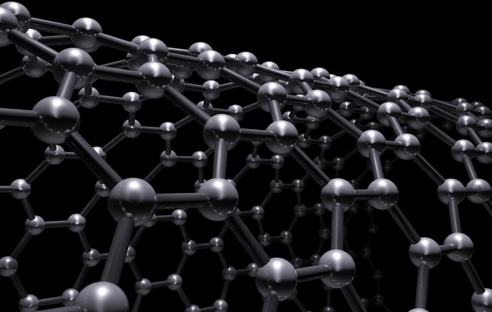
Carbon nanotubes are cylindrical nanostructures made by rolling up sheets of graphene. Graphene sheets are only a single atom thick and this gives this form of carbon many special properties. For example, graphene has excellent thermal and electrical conductivity. Electron mobility in graphene is higher than in the classic semiconductor material, silicon.
By shaping and manipulating graphene sheets into carbon nanotubes of different sizes and thicknesses, these properties can be tuned for particular applications. However, being able to characterize the nanotube size and shape is an essential part of the manufacturing process.
Optical microscopy is one of the most widely used imaging techniques for materials characterization. For conventional optical microscopes, the small size of carbon nanotubes makes them very challenging to image at a single-molecule level. The diffraction limit of optical light, which is one factor in determining the smallest distances that can be resolved by the microscope, is approximately equal to half the wavelength.
For visible light, this generally means it is difficult to distinguish objects smaller than 200 nm. A single-layered carbon nanotube may be as little as 0.4 nm in diameter so to use optical microscopy to image carbon nanotubes, a different approach is required than simply directly imaging the object with visible light.
Smaller Objects
One approach for imaging carbon nanotube, without resorting to electron microscopy techniques, is to ‘label’ them in some way. Methods have been developed to use gold or titanium dioxide nanoparticles to decorate the tubes.1,2 The strong scattering of visible light from the nanoparticles makes it possible to visualize even relatively small nanotubes.
However, such methods involve finding techniques to deposit the nanoparticles selectively onto the tubes that are compatible with the chemical environment of interest. Another problem with using ‘labels’ in this way, is that the interaction between the deposited material and the tube alters the properties of the carbon nanotube.3
Another high-throughput alternative for imaging carbon nanotubes with optical microscopy is to use a silicon wafer and etching with hydrogen fluoride.3 The nanotubes are deposited on the silicon surface and enhance the etching rate in regions where they are present. The greater rate of etching near the tubes creates trenches in the etched SiO2 layer that are viewable with optical microscopy techniques. This method has the advantage of being label-free and affordable but becomes cumbersome in terms of the sample preparation and imaging equipment required.
New Developments
New methodologies for using optical microscopy that are compatible with different sample types and environments are constantly being developed and this has meant optical microscopy has become an important tool in understanding the behavior and properties of these nanoscale systems.4
Being able to image at the single nanotube level in a non-invasive fashion is very important for understanding the structure-function relationships that govern the properties of nanotubes. While it is challenging to beat the exquisite spatial resolution that can be achieved with electron microscopy, optical microscopy still offers excellent sensitivity and it is considerably more straightforward to achieve good temporal resolution with optical microscopy than electron microscopy techniques.5
Optical microscopy is a broad term that encompasses many different techniques, including fluorescence, dark-field, and surface plasmon resonance microscopy. There are also now a series of super-resolution microscopy techniques that ‘beat’ the diffraction limit and resolve structures only a few nanometers in size.6
Super-resolution is not just a technique to look at carbon nanotubes but is a tool benefitting from the tunable optical properties of these nanostructures. Carbon nanotubes strongly absorb near-infrared radiation. With the addition of a photoswitchable molecular species to the nanotube, the system has sufficiently bright, controllable photoblinking properties to be used for super-resolution microscopy in the near-infrared.7 This is an important development for looking at biological samples as most tissues tend to have greater transparency and produce less scatter in this wavelength region.
Future Challenges
The potential applications for carbon nanotubes are seemingly endless.8 Be it for their outstanding tensile strength and potential as an alternative building material to steel or the ability to create long, exceptionally strong fibers9, carbon nanotubes are likely to remain a highly active area of research.
Another hope is that carbon nanotubes might be a building block not just of large-scale structures, but also electronic circuits. Carbon nanotubes have excellent optoelectronic properties that can be tuned by changing the diameter and length of the tube as well as the patterns of connectivity between the carbons.
Optical microscopy can be used to track the photoinduced behavior in the nanotubes and understand how the energy following light absorption propagates and quenches in the nanoscale structure.10 By combining such experiments with theoretical modeling, the structure-activity relationships that govern all of the nanotube properties can be investigated and we can start to understand some of the fundamental physics that make these systems so special.
References and Further Reading
- Liu, H., He, J., Tang, J., Liu, H., Pang, P., Cao, D., … Nuckolls, C. (2010). Translocation of Single-Stranded DNA Through Single-Walled Carbon Nanotubes. Science, 327, 64–68.
- Huang, S., Qian, Y., Chen, J., Cai, Q., Wan, L., Wang, S., & Hu, W. (2008). Identification of the structures of superlong oriented single-walled carbon nanotube arrays by electrodeposition of metal and raman spectroscopy. Journal of the American Chemical Society, 130(36), 11860–11861. https://doi.org/10.1021/ja803682j
- Novak, M. A., Surwade, S., Prokop, J., Bolotin, K., Hone, J., Brus, L., … Liu, H. (2014). Visualizing individual carbon nanotubes with optical microscopy. Journal of the American Chemical Society, 136(24), 8536–8539. https://doi.org/10.1021/ja503821s
- Wang, W. (2018). Imaging the chemical activity of single nanoparticles with optical microscopy. Chemical Society Reviews, 47(7), 2485–2508. https://doi.org/10.1039/c7cs00451f
- Armstrong, M. R., Boyden, K., Browning, N. D., Campbell, G. H., Colvin, J. D., DeHope, W. J., … Torralva, B. R. (2007). Practical considerations for high spatial and temporal resolution dynamic transmission electron microscopy. Ultramicroscopy, 107(4–5), 356–367. https://doi.org/10.1016/j.ultramic.2006.09.005
- Huang, B. (2010). Super-resolution optical microscopy: multiple choices. Current Opinion in Chemical Biology, 14(1), 10–14. https://doi.org/10.1016/j.cbpa.2009.10.013
- Godin, A. G., Setaro, A., Gandil, M., Haag, R., Adeli, M., Reich, S., & Cognet, L. (2019). Photoswitchable single-walled carbon nanotubes for super-resolution microscopy in the near-infrared. Science Advances, 5, IR 0 IR-ECP 4 60 g potential 5 1 823.5880147-0.15.
- Iijima, S. (2002). Carbon nanotubes: Past, present, and future. Physica B: Condensed Matter, 323(1–4), 1–5. https://doi.org/10.1016/S0921-4526(02)00869-4
- Bai, Y., Zhang, R., Ye, X., Zhu, Z., Xie, H., Shen, B., … Wei, F. (2018). Carbon nanotube bundles with tensile strength over 80 GPa. Nature Nanotechnology, 13(7), 589–595. https://doi.org/10.1038/s41565-018-0141-z
- Georgi, C., Böhmler, M., Qian, H., Novotny, L., & Hartschuh, A. (2009). Probing exciton propagation and quenching in carbon nanotubes with near-field optical microscopy. Physica Status Solidi (B) Basic Research, 246(11–12), 2683–2688. https://doi.org/10.1002/pssb.200982306
Disclaimer: The views expressed here are those of the author expressed in their private capacity and do not necessarily represent the views of AZoM.com Limited T/A AZoNetwork the owner and operator of this website. This disclaimer forms part of the Terms and conditions of use of this website.