The new TM4000 II benchtop SEM from Hitachi enables users to image and analyze any sample easily within a few minutes.
With the TM4000 II benchtop SEM, advanced electron microscopy becomes fast and easy for any user. High contrast, high resolution, fast identification of chemical element distribution, and large depth-of-focus imaging can be realized in minimal sample preparation time.
Key Features
- High-resolution imaging with magnification between 25x and 250,000x
- Users can quickly optimize their results with voltage control (up to 20 kV) and probe current control
- Thanks to the dedicated Secondary Electron (SE) detector, users can observe distinct topographical contrast
- The Backscatter Electron (BSE) detector supports fast identification of compositional change in the specimen
- Users can avoid charging issues on electrically insulating specimens by switching to vacuum mode in a single click
- Large or multiple specimens can be examined with the help of the large stage and chamber (samples with a diameter of up to 80 mm and a height of up to 50 mm)
- Users can navigate their sample fast with the built-in navigation camera and motorized stage*
- Users can gain a deeper chemical understanding by using the X-ray microanalysis (EDX) capability (option), which includes fast mapping*
- Microscopy and data analysis can be automated with options for multi-field acquisition and automated particle and phase analysis*
- Quantitative surface metrology data can be directly obtained in the SEM*
- Sophisticated detection capabilities such as STEM or Cathodoluminescence can be added*
- Dynamic experiments can be observed in-situ with heating, cooling, tensile or compression, nanoindentation, and electrical probing sub-stages*
*Options
Flexible Imaging Made Easy
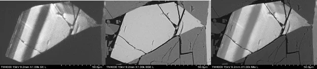
Usability and time-to-date form the core of the TM4000, but without affecting the versatility required to truly understand the sample. Users can choose between BSE (compositional contrast) and SE (surface contrast) on both insulating and conductive samples without the need for prior sample preparation.
Both BSE and SE detectors can be observed in parallel (combined or separately) and in low-vacuum mode. The potential to choose suitable acceleration voltage and probe current ensures that the most optimal results are achieved.
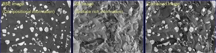
Left: Chemical contrast (BSE). Middle: Topography (SE). Right: Mixed SE/BSE image. Image Credit: Hitachi High-Tech Europe
Fast Navigation
Thanks to the completely integrated optical navigation camera, users can find their way around their specimen quickly. Users can easily overlay and correlate their SEM and optical images so that they know precisely where they are and what they have done at all times.
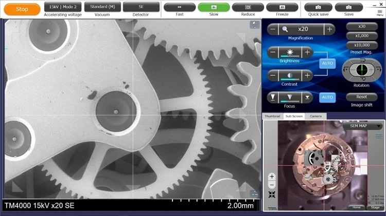
The left side shows an SE image of the inside of a watch, bottom right shows the optical image with overlaid SEM images from areas that have been imaged. Image Credit: Hitachi High-Tech Europe
High-Performance EDS for Advanced Elemental Analysis
The built-in X-ray microanalysis (EDS) system from pioneering suppliers such as Bruker or Oxford Instruments guarantees quick and precise elemental analysis with sophisticated features that are not available on other benchtop SEMs. Thanks to live peak deconvolution, spectral line overlaps are eliminated, thus offering true elemental distribution and preventing inadvertent misinterpretation.
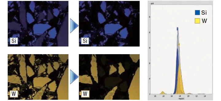
Line overlap with W and Si peaks in the spectra on the right. By using peak deconvolution, it is possible to see which grains actually contain W. Image Credit: Hitachi High-Tech Europe
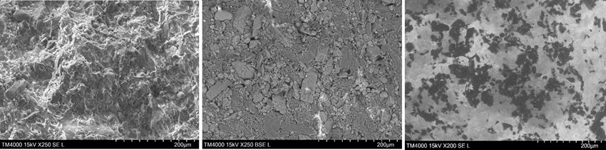
Automate Particle, Fiber, or Chemical Analysis
Robust modules can be added to automate users’ particle, matrix, or fiber analysis (a capability often linked to only full-size SEMs), thus enhancing users’ statistics and avoiding time-consuming work. Completely automated acquisition and analysis in the TM4000 allows morphology, size, and chemical composition to be characterized quickly, even over thousands or millions of features. This feature can play a vital role in the characterization of materials, such as:
- Metal powders for additive manufacturing
- Electrospun fibers
- Steel cleanliness (to ISO4967 standard)
- Technical cleanliness (to VDA19/ISO16232 standards)
- Identification, liberation, and characterization of the mineral phase
- Asbestos analysis (to VDI 3492/ISO14966 standards)
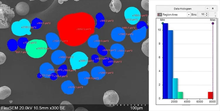
Left: Automatic particle detection. Right: Particle size distribution. Image Credit: Hitachi High-Tech Europe
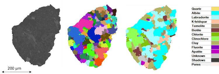
Mineral particle identification and characterization using Bruker AMICS. Left: BSE image. Middle: Identified particles. Right: Mineral classification. Image Credit: Hitachi High-Tech Europe
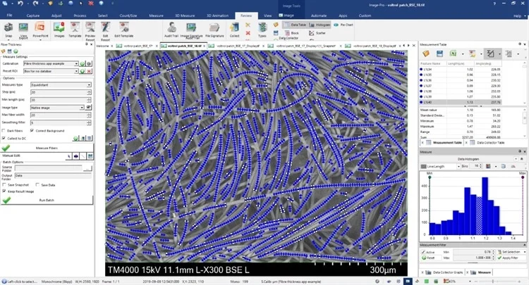
Automated fiber thickness measurement. Image Credit: Hitachi High-Tech Europe
Examine Wide Areas Automatically
Thanks to modules for completely automated wide-area acquisition and stitching (which includes imaging and chemical analysis), users can obtain all the required high-resolution data, even across huge length scales.
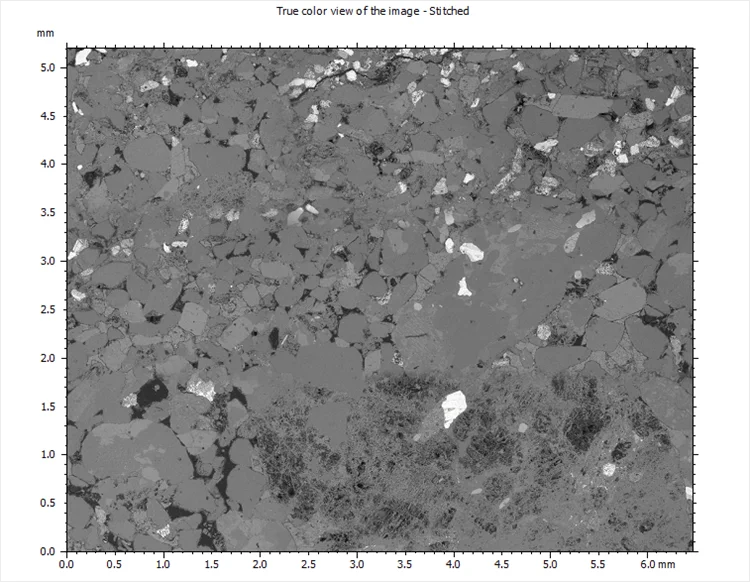
Geological thin section stitched using 3 x 3 images to cover a 6 x 5 mm area. Image Credit: Hitachi High-Tech Europe
Quantitative Surface Metrology
The built-in, tilt-free 3D surface modeling and metrology enables users to understand their material surfaces in detail. Surface parameters like angle, depth, or roughness — including 3D surface textures mentioned in ISO 25178 — can be measured.
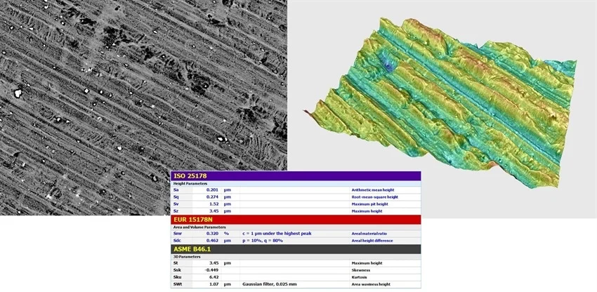
3D surface roughness of a worn metal surface. Image Credit: Hitachi High-Tech Europe
Cathodoluminescence Detector
The built-in cathodoluminescence detector can detect light emitted from different pharmaceutical, semiconductor, and geological materials in response to irradiation by an electron beam. This could prove to be a robust tool to locate active pharmaceutical ingredients (API) in pharma samples or to perform geological studies such as growth history and zonation of crystals.
Sample: Coarse-grained Syenite with zonation in the alkali feldspar. Left: CL image. Middle: BSE image. Right: Mixed CL and BSE. Small variations in Ca and Na content create CL contrast, hardly visible in the BSE image. Image Credit: Hitachi High-Tech Europe
SE, BSE, and CL images of a pharmaceutical powder. Image Credit: Hitachi High-Tech Europe
Scanning Transmission Electron Microscopy (STEM)
Users can image electron transparent samples like nanoparticles or biological sections with high contrast and remarkable ease than traditional SEM and TEM. For instance, the TM4000 can be employed for sample screening before high-throughput imaging of pigments in polymers, complete TEM examination, or analysis of graphene flake size.
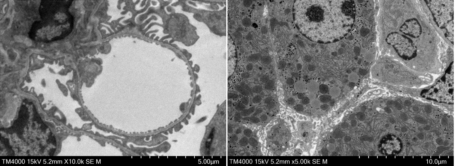
Left: Mouse kidney. Right: Mouse liver. Image Credit: Hitachi High-Tech Europe
In-Situ Testing
The TM4000 includes multiple options and accessories to allow in-situ experiments. In situ stages are provided for sample manipulation, tilting, tensile or compression testing, rotation, electrical probing, nanoindentation, fatigue testing, heating, cooling, etc.
Tensile test in SEM using Deben tensile tester
Example of tensile testing in the SEM, in this case of a leather sample. Video showing a Deben tensile test option. Video Credit: Hitachi High-Tech Europe