The Hitachi IM4000II and ArBlade 5000 ion milling systems deliver high-precision sample preparation for scanning electron microscopy. Whether working with metals, semiconductors, polymers, ceramics, or layered materials, these systems produce high-quality cross-sections and polished surfaces with minimal artifacts.
Engineered for academic research, industrial quality control, and materials science laboratories, both systems provide fast, consistent results - making them indispensable for advanced electron microscopy applications.
- High milling rate means fast and efficient sample preparation for hard materials
- Flexible options for various applications, including both cross-section and flat milling
- Optional cryogenic cooling is also available to reduce damage to temperature-sensitive samples
- With its user-friendly touchscreen interface, the system is easy to operate
- Optimized for both SEM and AFM, and is compatible with microscopes from both Hitachi and third-party manufacturers
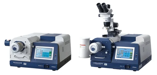
Image Credit: Hitachi High-Tech Europe
IM4000II
The IM4000II is a flexible, all-in-one system that provides both cross-section and flat milling, making it an ideal sample preparation tool for any lab.
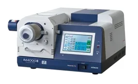
Image Credit: Hitachi High-Tech Europe
ArBlade 5000
The more advanced ArBlade 5000 features a higher milling rate and wide-area cross-section milling, making it perfect for demanding applications and labs that require high throughput.
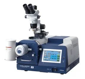
Image Credit: Hitachi High-Tech Europe
Features and Benefits
Fast and Precise Milling for a Wide Range of Materials
Reduce turnaround times without compromising sample integrity.
- The IM4000II achieves a 500 μm/hour milling rate, while the ArBlade 5000 offers an impressive 1 mm/hour or more (for Si samples with a 100 µm protrusion).
- This high-speed milling is perfect for hard materials like metals and semiconductors that require extended milling times.
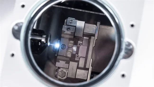
Image Credit: Hitachi High-Tech Europe
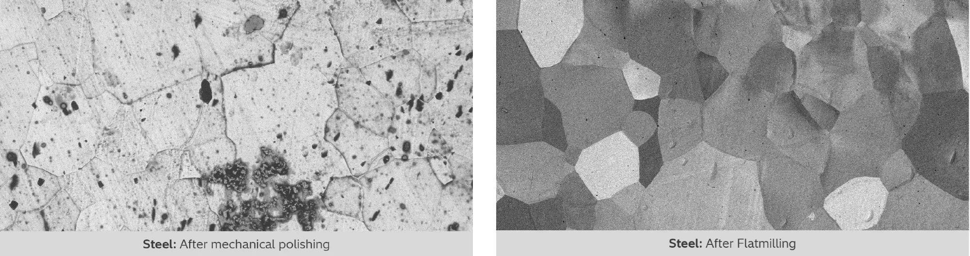
Cross-Section and Flat Milling for Flexible Sample Preparation
Users have the flexibility to prepare samples exactly how they need them.
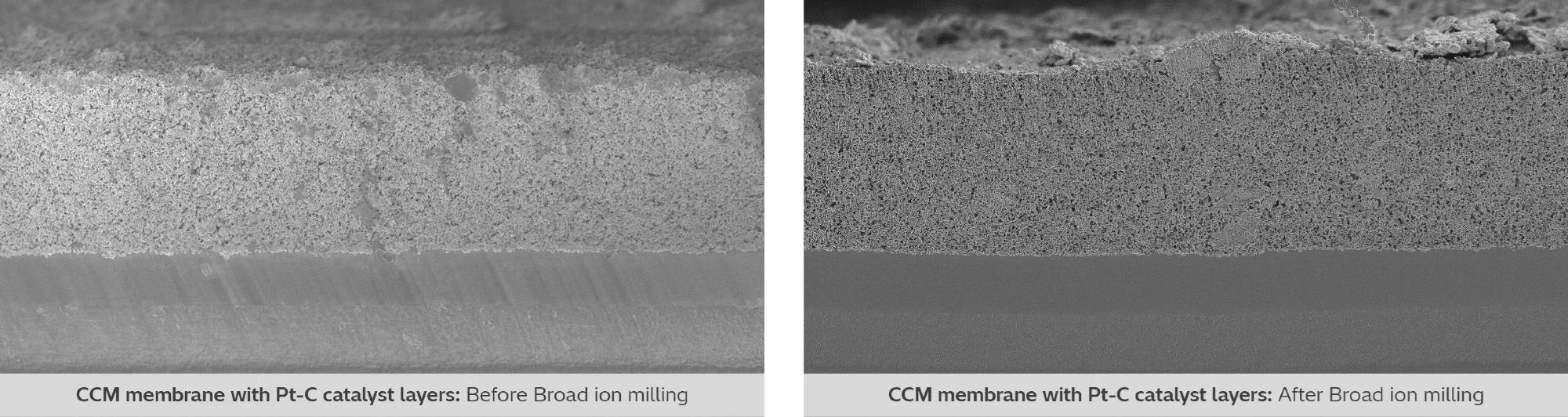
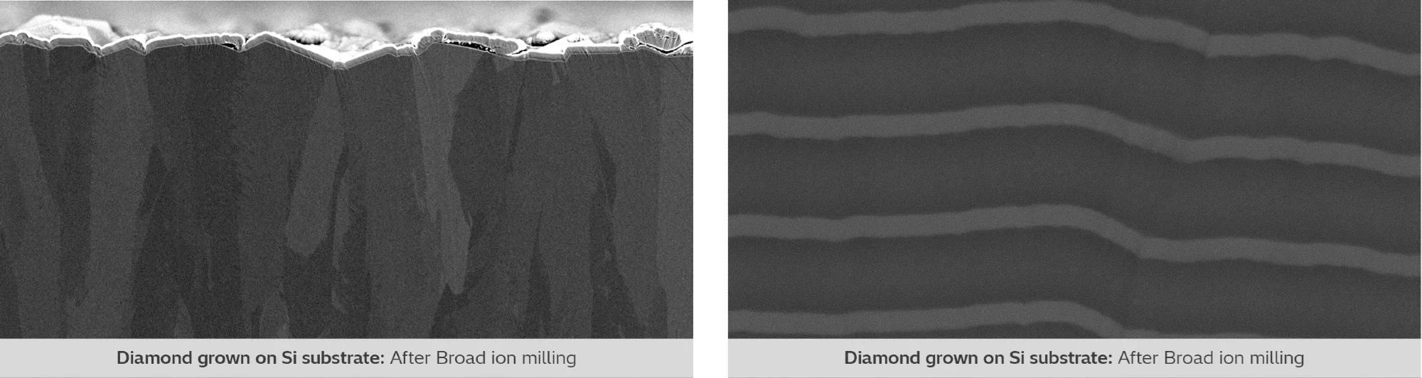
- Cross-section milling produces smooth, undistorted surfaces without introducing mechanical stress, making it ideal for examining the internal structures of composite materials, multilayer films, and electronic components.
- Flat milling eliminates surface layer artifacts, delivering clean, high-contrast imaging that is especially important for applications such as EBSD.
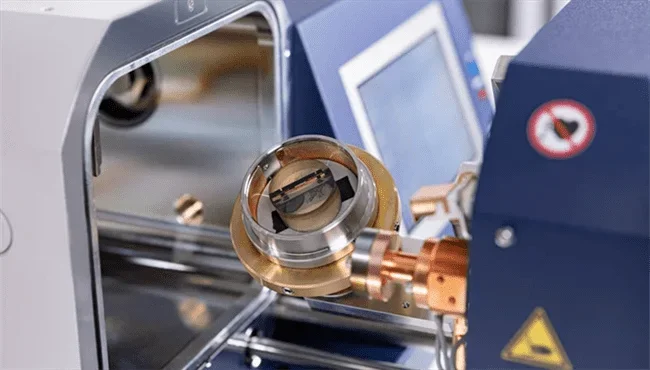
Image Credit: Hitachi High-Tech Europe
Wide-Area Cross-Section Milling (ArBlade 5000 Only)
Effortlessly prepare large samples with confidence.
- The system enables milling up to 10 mm in width, making it ideal for large electronic devices and industrial materials.
- Provides a uniform cross-section across the entire sample, which improves the accuracy of imaging and analysis.
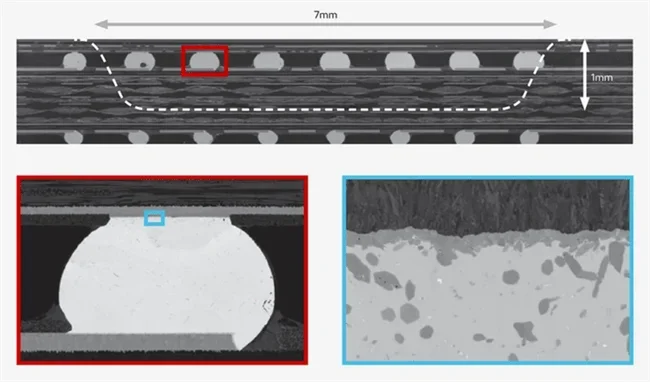
Image Credit: Hitachi High-Tech Europe
Cryogenic Cooling For Temperature-Sensitive Samples
Preserve sample integrity for high-resolution imaging.
- The optional Cooling Temperature Control function on the IM4000II and ArBlade 5000 protects sensitive materials (such as polymers) from heat-related damage.
- Maintains a precise temperature range (0 °C to -100 °C) using liquid nitrogen.
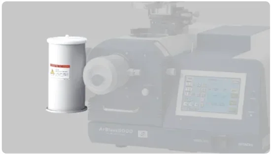
Image Credit: Hitachi High-Tech Europe
Seamless Integration With Scanning Electron Microscopes (SEMs)
Ensure contamination-free imaging for air-sensitive samples.
- The Air Protection Holder Unit, available for both the IM4000II and ArBlade 5000, allows the user to transfer samples to an SEM or AFM without exposure to air.
- Works seamlessly with Hitachi SEMs as well as external systems, ensuring efficient workflow integration.
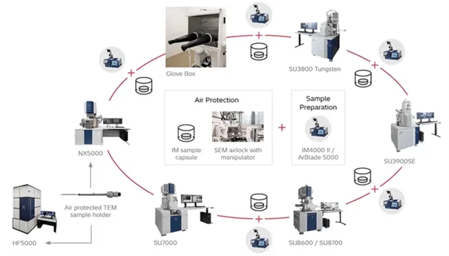
Image Credit: Hitachi High-Tech Europe
Applications Gallery
Metals and Alloys
Prepare cross-sections of hard materials for microstructural analysis. Image Credit: Hitachi High-Tech Europe
Batteries
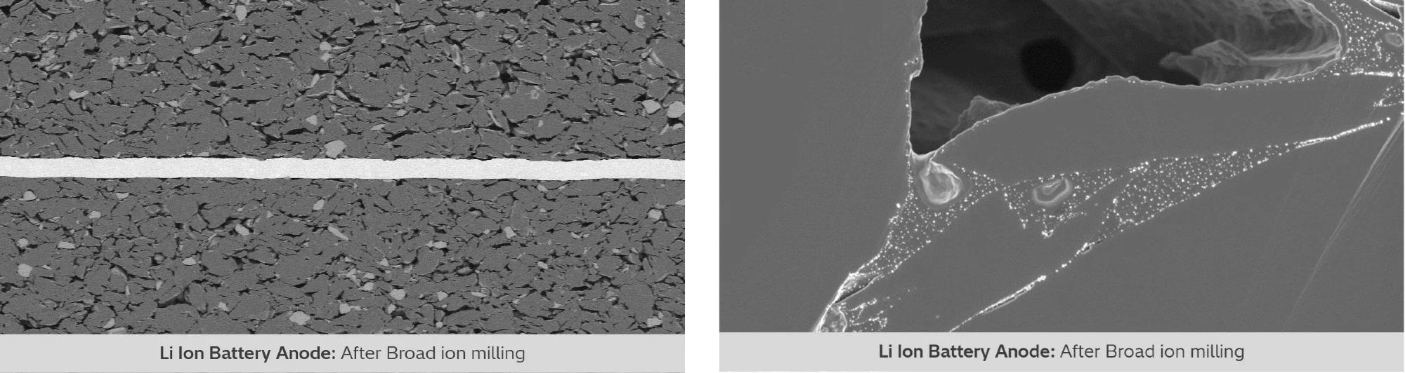
Cross-section of Li Ion Battery Anode. Image Credit: Hitachi High-Tech Europe
Electronics and Semiconductors
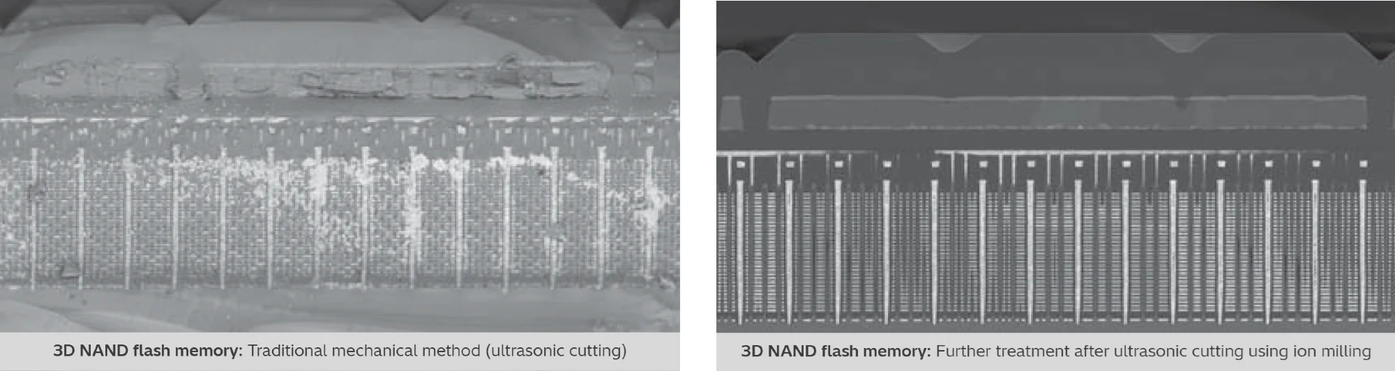
Expose layers and interfaces in integrated circuit. Image Credit: Hitachi High-Tech Europe
Polymers and Soft Materials
Prevent deformation in temperature-sensitive samples. Image Credit: Hitachi High-Tech Europe
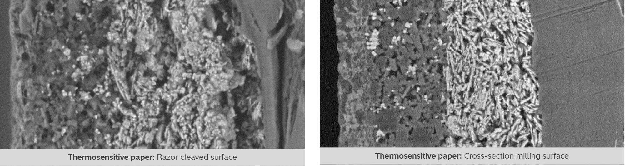
Multilayer Films and Coatings
Study layer composition and adhesion quality. Image Credit: Hitachi High-Tech Europe
Hard Materials
Cross-section milling example. Image Credit: Hitachi High-Tech Europe
Specifications
Source: Hitachi High-Tech Europe
| |
IM4000II |
ArBlade 5000 |
| Gas Used |
Ar (argon) gas |
Ar (argon) gas |
| Accelerating Voltage |
0 to 6 kV |
0 to 8 kV |
| Maximum Milling Rate (estimated for Si samples and 100 μm protrusion) |
500 μm/h or more |
≥ 1 mm/h |
| Maximum Milling Width |
Not available |
10 mm |
| Maximum Specimen Size |
20(W) x 12(D) x 8(H) mm |
20(W) x 12(D) x 8(H) mm |
| Sample Moving Range |
X: ±7 mm, Y: 0 to +3 mm |
X: ±7 mm, Y: 0 to +3 mm |
| Ion Beam Intermittent Irradiation |
ON/OFF setting (1 sec to 59 min 59 sec) |
Standard function |
| Swing angle |
±15 °, ±30 °, ±40 ° |
±15 °, ±30 °, ±40 ° |
| Wide-Area Cross-Section milling |
Not available |
Up to 10 mm width |
| Flat Milling Area |
φ 32 mm |
φ 32 mm |
| Maximum Flat-Milled Sample Size |
φ 50 x 25(H) mm |
φ 50 x 25(H) mm |
| Rotation Speed |
1 rpm, 25 rpm |
1 rpm, 25 rpm |
| Tilt Range |
0 to 90 ° |
0 to 90 ° |
| Cooling Temperature Control (optional) |
0 to -100 °C via LN2 |
0 to -100 °C via LN2 |
| Higher Beam Tolerance Mask (optional) |
2x beam tolerance (Cobalt-free) |
2x beam tolerance (Cobalt-free) |
| Stereo Microscope Unit (optional) |
15x to 100x, Binocular/Trinocular |
15x to 100x, Binocular/Trinocular |