The Cold Field Emission source is well-suited for high-resolution imaging, thanks to its small source size and low energy spread. Hitachi’s innovative CFE Gun technology enhances beam brightness and stability, enabling both high-resolution imaging and high-quality elemental analysis.
To support stable data acquisition at the instrument’s peak performance, the SU9000II introduces new features that automate optical system adjustments. Paired with the optional EM Flow Creator software, users can also automate data acquisition - particularly for sequential data collection.
Additionally, the SU9000II’s unique optical system design supports EELS, expanding its capabilities for advanced material analysis.
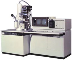
Overview
The SU9000II is Hitachi’s latest premium SEM, designed with unique electron optics that place the sample within the gap between the upper and lower sections of the objective lens pole piece.
This true in-lens configuration, combined with Hitachi’s next-generation cold field emission technology, delivers exceptional system resolution and stability. It achieves secondary electron (SE) resolution of 0.4 nm at 30 kV and 0.7 nm at 1.0 kV (with the deceleration feature option), offering top-tier performance for high-precision imaging.
New Coherent Cold Field Emission Source
To ensure this level of resolving power is practical for everyday lab use, the SU9000II is equipped with an ultra-stable side-entry sample stage - similar to those found in high-end TEM systems. It also features optimized vibration damping and a fully enclosed cabinet to shield the electron optics from environmental noise.
In addition, the SU9000II’s clean vacuum design delivers a vacuum level in both the gun and sample chamber that is an order of magnitude better than the previous generation. This helps minimize sample contamination artifacts. For even cleaner results, pre-observation sample cleaning can be carried out using Hitachi’s ZONESEM sample cleaner.
Sample Cleaner ZONESEMⅡ
To allow for stable data acquisition at the instrument’s highest performance levels, the SU9000II offers new capabilities that render automated adjustments of the optical system, and the new EM Flow Creator software package as an option to render automated data acquisition, particularly sequential data collection.
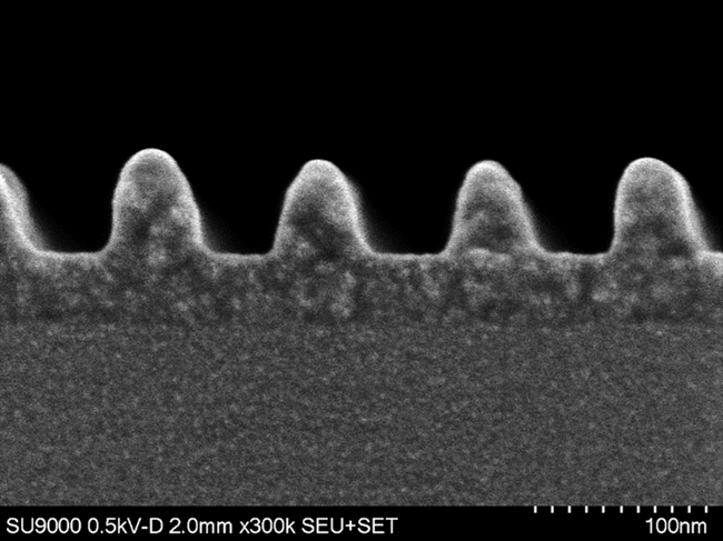
Sample: ArF Resist; Vacc: 500 V; Signal: SE image; With beam deceleration. Image Credit: Hitachi High-Tech Europe
In addition to delivering exceptional resolution, the SU9000 is equipped with a versatile 2+2 detection system designed for surface, composition, and transmission imaging.
The patented Super ExB filter, used in combination with the upper detector, allows users to isolate and collect SE and low-angle BSE signals of interest. This helps suppress charging artifacts while highlighting surface topography.
The top detector, on the other hand, selectively captures high-angle BSE signals, providing topography-free information related to material composition and crystallographic orientation. This advanced signal selection makes the SU9000 especially valuable for catalyst research and for biological and pharmaceutical immunolabeling, particularly when paired with a cryogenic sample holder.
The SU9000 also functions as a highly capable low-kV STEM, often delivering better contrast on critical features than high-energy S-TEM systems. It supports simultaneous brightfield and annular darkfield imaging, with the darkfield detector adjustable to 56 different positions, allowing precise tuning of Z-contrast for the structure or material of interest.
Application in Bulk Specimens
Acquisition of Multiple Surface Information of Catalyst (Gold/Alumina Carrier) Specimen Using Top and Upper Detector
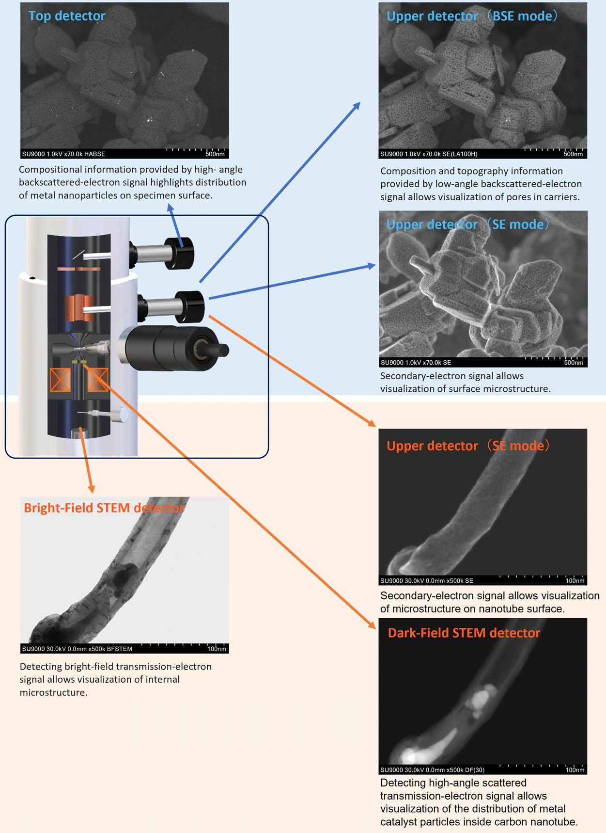
Image Credit: Hitachi High-Tech Europe
Application of Nanomaterials and Thin Films
Simultaneous multiple signal collection of SE, BF- STEM, and DF-STEM signals was demonstrated in imaging of a multi-walled carbon nanotube.
The exceptional stability of the SU9000 supports a guaranteed STEM resolution of 0.34 nm, making it possible to observe fine structural details - such as graphite lattice fringes within a carbon nanotube - with confidence and clarity.
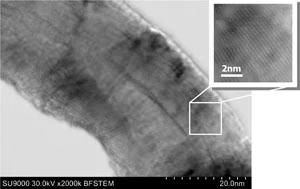
Sample: Multi wall carbon nano tube (lattice fringes); Vacc: 30 kV; Mag.: 2,000kx; Bright Field(BF)-STEM image. Image Credit: Hitachi High-Tech Europe
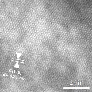
Sample: Graphene (lattice fringes); Vacc: 30 kV; Mag.: 3,000kx; Bright Field(BF)-STEM image. Image Credit: Hitachi High-Tech Europe
Features
- Advanced vacuum technology achieves ultra-high vacuum (UHV) levels, significantly reducing sample contamination
- A newly designed Cold Field Emission (CFE) gun delivers high brightness and exceptionally stable emission current
- Highly engineered instrument enclosure provides exceptional strength and stability, enabling high-resolution imaging across a wide range of environmental conditions
- New capabilities allow automated adjustments of the optical system, while an optional feature enables automated data acquisition - ideal for sequential data collection
- Newly designed CFE GUN provides high brightness and an extremely stable emission current
- Redesigned objective lens supports high-resolution imaging even at low accelerating voltages
- Side-entry sample exchange system boosts throughput by reducing sample change time and automatically aligning the sample to the current working distance.
- Outstanding low-kV performance makes it ideal for imaging beam-sensitive materials, with guaranteed SE resolution of 0.7 nm at 1.0 kV (using the deceleration feature)
- Highest guaranteed SE resolution of 0.4 nm at 30 kV
- Usable magnification range up to 3,000,000x
In-Lens SEM
Launched in 1986 with 1000 units installed, the Hitachi S-900 was the world’s first commercial in-lens field emission SEM (FE-SEM). Offering 0.8 nm SE resolution and a usable magnification of up to 800,000x, the S-900 introduced a groundbreaking concept that opened up new possibilities for researchers across a wide range of disciplines.
Following the success of the S-900, Hitachi continued to set new standards with the release of the S-5000 in 1990, the S-5200 in 2000, and the S-5500 in 2004.
In 2011, to celebrate 25 years of its in-lens FE-SEM technology, Hitachi introduced the SU9000, which became the most powerful member of its high-end product line.
Hitachi S-900 (1986). Image Credit: Hitachi High-Tech Europe
LV-STEM
High-Resolution, Analytical STEM/SEM Offering Simultaneous Chemical and Bonding Analysis, Atomic Resolution, and Surface Imaging at 30 kV and Below
Exploring the full capabilities of STEM at 30 keV and below has become a rapidly growing focus in both Materials and Life Sciences. This low-voltage STEM (LV-STEM) approach brings together SEM and STEM functionality, including EDX and EELS, at low beam energies, where reduced beam damage and enhanced contrast are major advantages.
Historically out of reach for many researchers, LV-STEM now makes it possible to investigate biological materials in an unstained state with unprecedented clarity.
Unlike TEM, STEM imaging does not rely on post-sample imaging lenses. This means inelastically scattered electrons don’t significantly degrade image quality - an effect that becomes even more meaningful at lower voltages, where chromatic aberrations typically increase. As a result, samples that would traditionally require at least a 100-keV TEM can now be examined using low-keV STEM.
While multi-scattering and absorption still limit the maximum acceptable specimen thickness, the use of advanced sample preparation or naturally thin specimens - as is common in nanotechnology - allows 30-keV STEM to cover many applications previously reserved for high-voltage TEM, while also providing surface information through standard SEM modes such as SE, BSE, and high-angle BSE.
Hitachi’s proven cold field emission gun (CFEG), a core component of its high-end SEMs, significantly enhances both STEM resolution and EELS capabilities. Even at unusually low voltages, the system achieves better than 400-meV FWHM for the zero-loss peak (ZLP) in EELS, enabling detailed fine structure analysis.
For example, subtle variations in π-bonding as layers are added to graphene can be clearly resolved - highlighting the system’s sensitivity. The LV-STEM includes a second, dedicated 3-element EELS detector that enables rapid (up to 10,000 fps) acquisition of energy-filtered BF STEM images, plasmon imaging, or fast elemental mapping. Switching between detectors is seamless, thanks to Hitachi’s uniquely integrated design.
The LV-STEM mode (Figure 2) complements SE imaging without compromise. Even without Cs or Cc correction, typical 30 keV images can achieve ~0.2 nm resolution, making the LV-STEM a true leader in ≤30 keV microscopy. The ability to capture STEM and SE data simultaneously ( as shown in Figure 3) further enhances the versatility and depth of information.
Additionally, the microscope supports samples up to 5.0 mm × 9.5 mm × 3.5 mm. The optional windowless EDX detector enables analysis of both thin and bulk regions. With an impressive collection angle of 0.7 sr, EDX map acquisition times are drastically reduced (see Figure 4 for details), making the LV-STEM a powerful tool across both materials and life sciences.
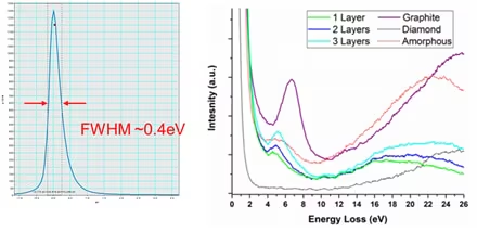
Figure 1. Left: despite the low (± 30 keV) energy of these electrons, the energy spread of the electron beam, measured by our own Hitachi EELS is 400 meV or less:. Right: EELS spectra differentiating between single, double and triple layers of graphene, graphite, diamond, and amorphous carbon. Image Credit: Hitachi High-Tech Europe
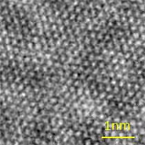
Figure 2. The low-pass-filtered BF STEM of Graphene at 30 keV shows a resolution of close to 0.2 nm; the 0.142 nm atom distances are not resolved. Image Credit: Hitachi High-Tech Europe
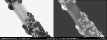
Figure 3. Left: The high-resolution 30-keV BF STEM image by itself makes it difficult to model its 3D structure. Right: Only in combination with the (simultaneously acquired) high-resolution SE image, the real structure of this sample becomes obvious and modeling this structure as a 3D model would be quite manageable. Image Credit: Hitachi High-Tech Europe
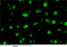
Figure 4. Elemental EDX map (Au M) at 30 kV. The size of the nano-particles is in the range of 5-10 nm. Acquisition time is 3.5 min at a current of 1 nA. Image Credit: Hitachi High-Tech Europe