FIB-SEM systems have become essential tools for characterizing and analyzing advanced technologies and high-performance nanoscale materials. As the demand for ultrathin TEM lamellae continues to grow, so does the need for ion and electron optics that can deliver high-quality results without introducing artifacts during FIB processing.
Hitachi’s NX2000 combines high-performance FIB capabilities with high-resolution SEM in a single system. With its unique sample orientation control* and triple beam* technologies, the NX2000 supports high-throughput, high-quality TEM sample preparation, making it a strong choice for today’s most demanding applications.
* Optional
Features
High-contrast, real-time SEM end-point detection enables ultrathin TEM sample preparation for sub-20 nm devices.
- Real-time SEM monitoring during FIB milling
- Sample: NAND flash memory
- Accelerating voltage: 1 kV
- Field of view (FOV): 0.6 µm
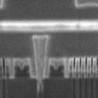
Real-time SEM monitoring during FIB milling; Sample: NAND flash memory; Accelerating voltage: 1 kV; FOV: 0.6 µm. Image Credit: Hitachi High-Tech Europe
Micro sampling* and a high-precision positioning mechanism* enable precise sample orientation control, supporting Anti-Curtaining Effects (ACE function) and the preparation of uniformly thick lamellae.
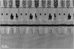
With sample orientation control. Image Credit: Hitachi High-Tech Europe
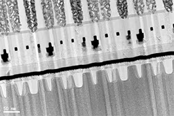
Without sample orientation control. Image Credit: Hitachi High-Tech Europe
Triple Beam system* Triple beam configuration for Ga FIB-induced damage reduction.
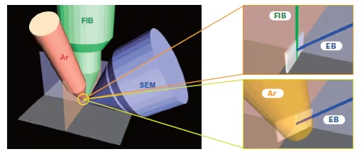
EB: Electron Beam; FIB: Focused Ion Beam; Ar: Argon ion beam. Image Credit: Hitachi High-Tech Europe
Specifications
Source: Hitachi High-Tech Europe
| FIB column |
| Resolution (SIM) |
4 nm @ 30 kV, 60 nm @2 kV |
| Acceleration voltage |
0.5 kV - 30 kV |
| Beam current |
0.05 pA - 100 nA |
| FE-SEM column |
| Resolution |
2.8 nm @ 5 kV, 3.5 nm @ 1 kV |
| Acceleration voltage |
0.5 kV - 30 kV |
| Electron source |
Cold cathode field emission source |
| Detector |
| Standard detector |
Upper/Lower SED & BSED |
| Stage |
X: 0 - 205 mm
Y: 0 - 205 mm
Z: 0 - 10 mm
R: 0 - 360 ° infinite
T: -5 - 60 ° |
Special Accessories (Optional)
- Air protection holder
- Ar/Xe ion 3rd column
- Automatic TEM sample preparation software
- CAD navigation software
- Cooling holder
- Double tilt system
- EDS (Energy Dispersive x-ray Spectroscopy) system
- Linkage software with defect inspection instruments
- Micro-sampling System
- Multi-gas injection system
- Plasma cleaner
- Swing function ( for Ar/Xe ion 3rd column)
- TEM sample preparation wizard
Application Data
Semiconductor
3D Reconstruction from Serial Section SEM Images
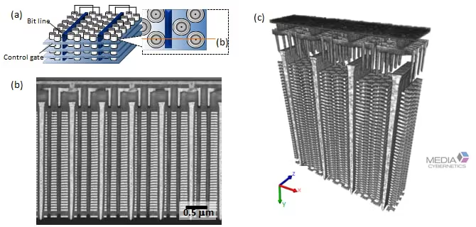
Specimen: 3D NAND flash memory. (a) Schematic view. (b) Cross-sectional BSD image (Accelerating voltage: 2 kV). (c) 3D reconstructed image (Volume rendering). Image Credit: Hitachi High-Tech Europe
Curtain Effect Free Lamella Preparation Using Double Tilt System
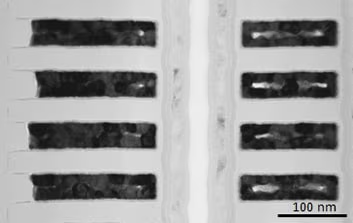
Specimen: 3D NAND flash memory; Observation: HF-3300 Cold FE-TEM (Accelerating voltage: 200 kV). Image Credit: Hitachi High-Tech Europe
High-Precision Site-Specific Lamella Preparation
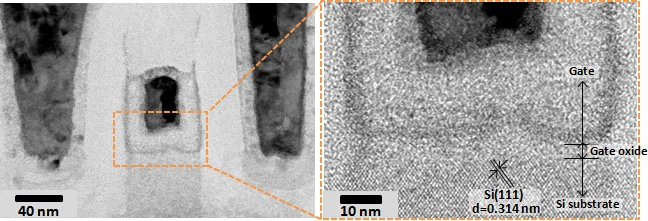
Specimen: 22 nm FinFET; Observation: HF-3300 Cold FE-TEM (Accelerating voltage : 200 kV). Image Credit: Hitachi High-Tech Europe
High-Quality Lamella Preparation With In-Situ Ar Ion Milling
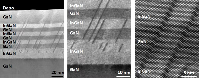
Specimen: GaN/InGaN; Final milling: 1 kV Ar; Observation: HD-2700 Aberration -corrected STEM (Accelerating voltage : 200 kV). Image Credit: Hitachi High-Tech Europe
Material Science
High-Quality Lamella Preparation With In-Situ Ar Ion Milling (1)
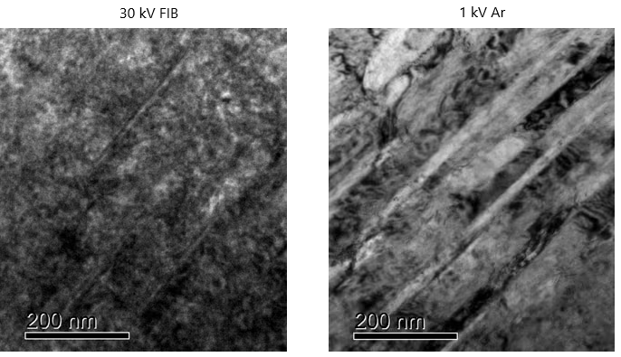
Specimen: Zirconium; Observation: HF-3300 cold FE-TEM (Accelerating voltage: 300 kV). Image Credit: Hitachi High-Tech Europe
High-Quality Lamella Preparation With In-Situ Ar Ion Milling (2)
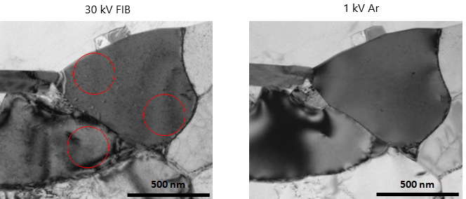
Specimen: Aluminum; Observation: HF-3300 cold FE-TEM (Accelerating voltage: 300 kV). Image Credit: Hitachi High-Tech Europe