Hitachi’s newly developed NX9000 FIB-SEM system features an optimized layout designed for true high-resolution serial sectioning, meeting the latest demands in 3D structural analysis as well as TEM and 3DAP studies. The NX9000 delivers exceptional precision in material processing, making it highly versatile for applications spanning advanced materials, electronic devices, biological tissues, and many other research areas.
Features
- The SEM and FIB columns are arranged orthogonally to optimize their positioning for high-resolution 3D structural analysis.
- This system also features a high-brightness cold-field-emission electron source and high-sensitivity optics, which support the analysis of a wide range of materials, from biological tissues to magnetic materials.
- The Micro-sampling and Triple Beam systems ensure high-quality sample preparation for both TEM and atom-probe applications.
Ion Milling and Observation at Normal Incidence in Real-Time for True Analytical Imaging
The SEM and FIB columns in the NX9000 are arranged orthogonally, enabling normal-incidence SEM imaging of FIB cross sections.
This orthogonal configuration eliminates issues such as aspect deformation, foreshortening of cross-sectional images, and field-of-view (FOV) shifts during serial section imaging—problems that are unavoidable with conventional FIB-SEM systems. As a result, the NX9000 provides highly accurate 3D structural analysis. In addition, its surface-planar EM imaging design makes it easy to integrate optical correlative microscopy.
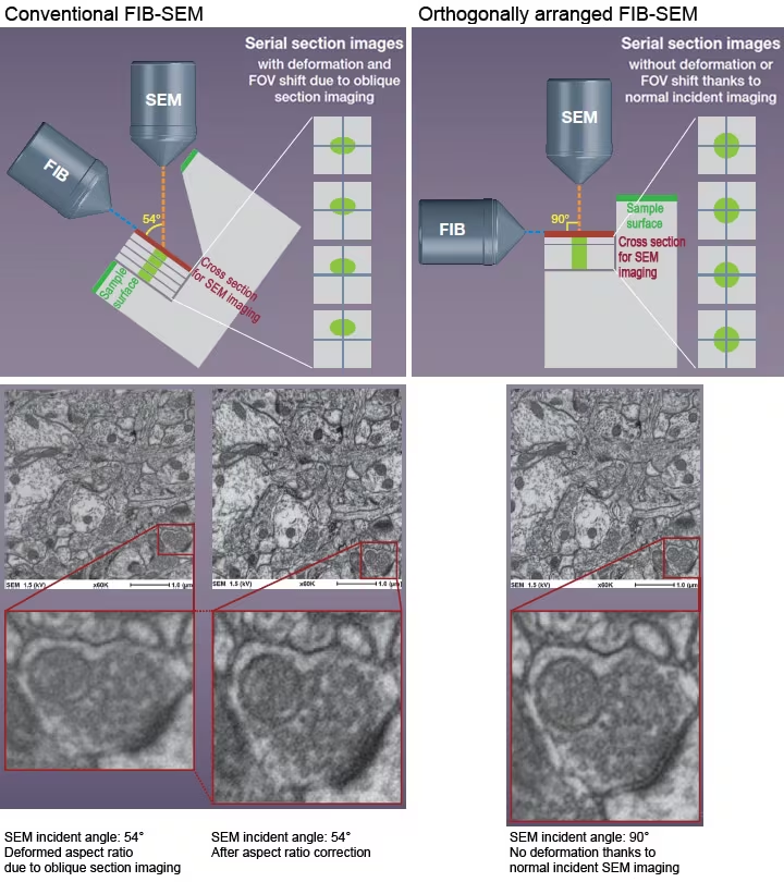
Sample: Mouse brain neuron; Sample courtesy of Yoshiyuki Kubota, Ph.D., Neural Information Processing Systems (NIPS). Image Credit: Hitachi High-Tech Europe
Cut & See·3D-EDS·3D-EBSD Available for a Wide Variety of Materials
Cut & See
Cut & See enables high-resolution, high-contrast imaging of biological tissues, semiconductors, and magnetic materials such as steel and nickel at low accelerating voltages. Thanks to the optimized geometry of the ion and electron columns, serial section images can be collected with high throughput.
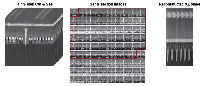
Sample: NAND flash memory; SEM accelerating voltage: 1 kV; Cutting interval: 1 nm; Number of cut: 300. Image Credit: Hitachi High-Tech Europe
3D-EDS
Serial section SEM images and elemental maps can be acquired using 3D-EDS. The large-area silicon drift detector shortens acquisition time and makes elemental mapping possible even at low accelerating voltages.
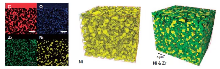
Sample: Fuel cell electrode; SEM accelerating voltage: 5 kV; Cutting interval: 100 nm; Number of cut: 212; Sample courtesy of Prof. Naoki Shikazono, University of Tokyo. Image Credit: Hitachi High-Tech Europe
3D-EBSD
Simultaneous SEM, FIB, and EBSD signals can be acquired for 3D-EBSD without the need to move the stage during FIB sectioning and EBSD analysis. This approach improves both accuracy and throughput, delivering high-quality 3D crystal orientation analysis and segmentation with minimal post-processing correction.
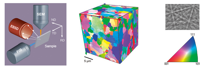
Sample: Ni; SEM accelerating voltage: 20 kV; Cutting interval: 150 nm; Number of cut: 150. Image Credit: Hitachi High-Tech Europe
Specifications
Source: Hitachi High-Tech Europe
| Items |
Description |
| SEM |
Electron source |
Cold cathode field emission source |
| Accelerating voltage |
0.1 - 30 kV |
| Resolution |
2.1 nm @ 1 kV |
| 1.6 nm @ 15 kV |
| FIB |
Ion source |
Ga liquid metal ion source |
| Accelerating voltage |
0.5 - 30 kV |
| Resolution |
4.0 nm @ 30 kV |
| Maximum probe current |
100 nA |
| Standard detector |
In-column SED/In-column BSED/Chamber SED |
| Stage |
X |
0 - 20 mm |
| Y |
0 - 20 mm |
| Z |
0 - 20 mm |
| θ |
0 - 360 ° |
| τ |
-25 - 45 ° |
| Maximum sample size |
6 mm x 6 mm, 2 mm thick |
Application Data
Material Science
3D Distribution Analysis With Multiple Signals
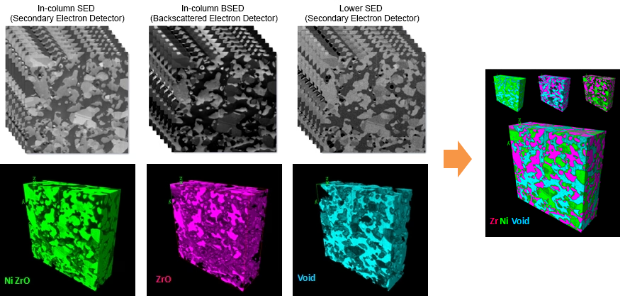
Specimen: Fuel cell electrode SEM accelerating voltage: 0.3 kV; FOV: 20 µm; Cutting interval: 10 nm; Number of cut: 600. Image Credit: Hitachi High-Tech Europe
Semiconductor
3D Structural Analysis from Serial Section SEM Images
Specimen: 3D NAND flash memory. Video Credit: Hitachi High-Tech Europe
High-Precision Site-Specific Lamella Preparation
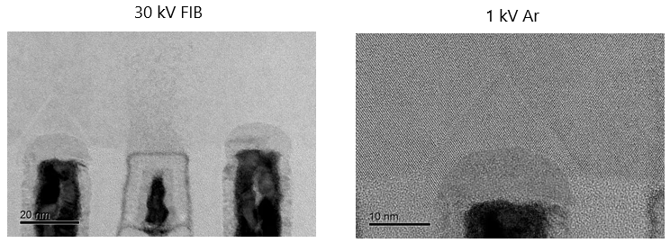
Specimen: 14 nm SoC device; Final milling: 1 kV Ar; Observation: HF-3300 Cold FE-TEM (Accelerating voltage: 300 kV). Image Credit: Hitachi High-Tech Europe
Life Science
3D Reconstruction from Serial Section SEM Images
Specimen: Mouse brain neuron. Video Credit: Hitachi High-Tech Europe