The SU8600 is a specialized imaging SEM that uses Hitachi’s cold field emission (CFE) technology to provide ultra-high resolution. Developed to satisfy the demands of industrial users, lab managers, and research scientists, the SU8600 CFE-SEM offers top-notch automation and spatial resolution for contemporary labs.
One monitor can show one, two, four, or six signals simultaneously. The dual-monitor setup widens the workspace and increases productivity by adding a second screen. Users can also customize the operation panel with dual monitors by placing submenus anywhere on each screen.
- Ultra-high resolution of 0.6 nm at 15 kV and 0.7 nm at 1 kV
- Sophisticated automation for reliable, repeatable processes
- Display up to six imaging signals at the same time
- Specimen loading through a typical six-inch exchange chamber is quick and simple
Features and Benefits
Ultra-High Resolution for Unmatched Imaging
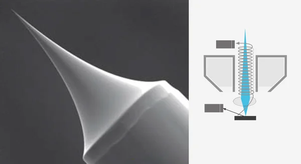
Image Credit: Hitachi High-Tech Europe
Even at low voltages, the SU8600's high-brightness cold-field emission source offers remarkable resolution. This makes it perfect for biological analysis, semiconductor research, and advanced material science, as it makes it possible to clearly record minute features.
The small energy width (nearly monochromatic) emission lowers chromatic aberrations, allowing users to use the SU8600 without beam boosting.
The magnetic lens field collects multiple signals generated by the observed specimen and guides them into the in-column multi-detector system. This device allows users to display up to six imaging signals simultaneously.
Smart Detector System for Better Contrast
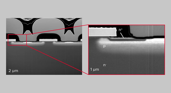
Image Credit: Hitachi High-Tech Europe
The Out-Column Crystal Type BSED (OCD) allows for rapid backscattered electron imaging (BSE), collecting structural details in under a second. Users can save time while accurately recognizing material variations, such as oxide and nitride layers in semiconductors.
High-pass filtering for elastically backscattered electrons enables material contrast imaging without requiring extensive beam penetration. Users can retain sample integrity while viewing surface-level characteristics, which is especially important for delicate specimens or beam-sensitive materials.
Energy filtering also provides the following benefits:
- Users can avoid image charging by selecting quicker, non-charge-affected electrons
- The user can visualize surfaces with varying conductivities, such as doping areas in semiconductors
- In addition to elastically backscattered electrons (material contrast information), users can simultaneously scan SE or filtered-SE (fine surface detail)
- Users can use a windowless EDS system at any accelerating voltage since the magnetic field prevents backscattered electrons from hitting the EDS detector and causing a spectrum background
Enhanced Automation for Reproducibility

Image Credit: Hitachi High-Tech Europe
The optional EM Flow Creator software allows users to organize SEM procedures into repeatable workflows using a “drag and drop” interface. Once a recipe has been defined, automated data collection under certain conditions can be performed with great precision and reproducibility. Users achieve reliable results with minimum manual involvement, making it ideal for labs conducting high-throughput trials.
Flexible and User-Friendly Design
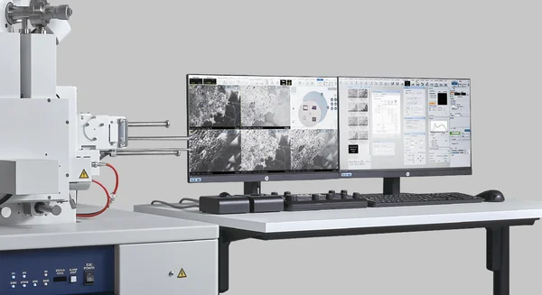
Image Credit: Hitachi High-Tech Europe
Up to six signals can be displayed simultaneously on a single display for quick data analysis. Alternatively, a dual monitor arrangement can increase the workspace with more display possibilities.
The conventional six-inch specimen exchange chamber, with an optional inert-gas transfer mechanism, allows users to reduce contamination concerns while accommodating a wide range of sample types.
Using the exchange chamber allows users to maintain the chamber continually under vacuum, resulting in minimum background contamination. The stage has a 110 mm × 110 mm range of motion in X and Y.
Specifications
Source: Hitachi High-Tech Europe
| Electron Optics |
| Resolution |
0.6 nm @ 15 kV, 0.7 nm @ 1 kV |
| Magnification |
20 to 2,000,000x |
| Voltage Range |
0.5 to 30 kV |
| Specimen Stage |
| Stage Control |
Motorized 5-axis control |
| X/Y/Z range |
0–110 mm / 1.5–40 mm |
| Tilt |
-5 ° to 70 ° |
| Detectors |
| Standard Detectors |
Optional Detectors |
| Upper Detector (UD) |
Top Detector (TD)
In Column Middle Detector (IMD)
Photo Diode BSE (PD-BSE)
Out Column Detector (OCD)
Bright Field TE (BFSTEM)
Dark Field TE (DFSTEM)
Cathodoluminescence Detector (CL)
EDS, EBSD |
| Lower Detector (LD) |
|
| Optional Accessories |
EDS and EBSD |
Applications Gallery
Material Science
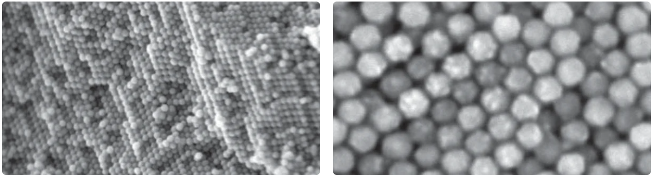
Self-Assembling Magnetic Iron Oxide Nanoparticles. Image Credit: Hitachi High-Tech Europe
Life Science
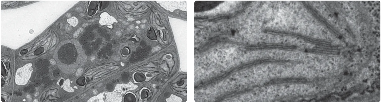
Ultrastructure of Arabidopsis. Image Credit: Hitachi High-Tech Europe
Semiconductor

Cross-Section Images of 3D NAND. Image Credit: Hitachi High-Tech Europe