The EDAX Clarity is the world’s first and only commercially available electron backscatter diffraction (EBSD) detector with unrivaled performance down to 3 kV. This technique is suitable for ceramic, beam-sensitive perovskite, or semiconductor materials that are difficult to analyze with conventional EBSD systems.
This groundbreaking series leverages single-electron detection to provide users with high-fidelity EBSD pattern quality and unparalleled sensitivity.
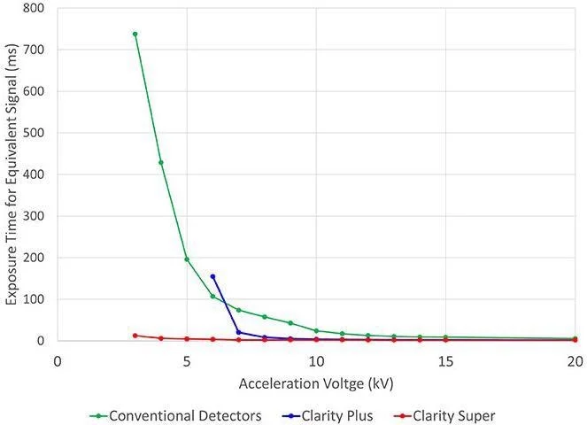
- Clarity Plus – Effective collection down to voltages of ~7 kV
- Clarity Super – Designed to work well at low voltages as low as 3 kV
Clarity uses an advanced hybrid-pixel direct detection technique with single-electron detection sensitivity.
During impact, the incident electrons form many electron-hole pairs inside the silicon, and a bias voltage transmits the charge to the underlying CMOS detector, which counts each event. Individual electrons can be identified with this method, whereas traditional EBSD detectors that use light transfer devices or phosphor screens cannot.

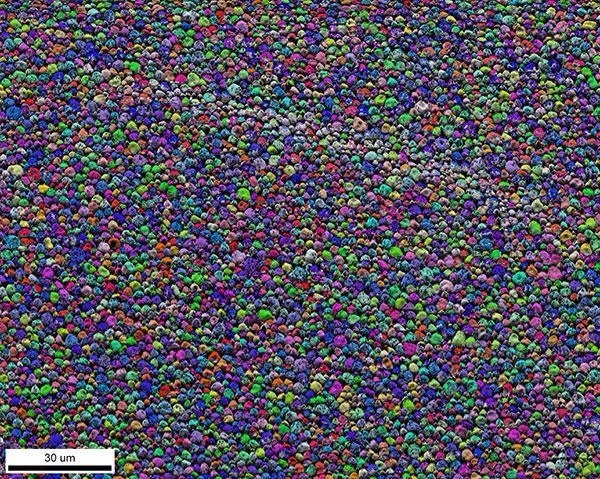
EBSD image quality and IPF orientation map from beam-sensitive MAPI perovskites collected at 10 kV and 150 pA beam dose. Image Credit: Gatan
Clarity delivers unmatched image quality and sensitivity thanks to virtually zero read noise. It is capable of detecting and analyzing patterns with fewer than 10 e-/pixel. This makes Clarity ideal for applications like hybrid organic-inorganic perovskite solar cells and ceramics that have low beam needs, as well as materials that are sensitive to beams.
Additionally, Clarity Super excels at lower kV acquisition, which improves spatial resolution for materials with fine-grained materials.

Sensitivity comparison of Clarity with conventional phosphor-based detectors. Image Credit: Gatan
Features and benefits
Beam sensitive materials analysis
- Low-vacuum SEM settings or conductive coatings are not required to investigate non-conductive materials like ceramics that conduct under conventional beam currents.
- Operating at low beam currents and energies reveals previously unseen structures while preventing sample damage.
- Captures high-quality EBSD patterns and maps at low beam currents to investigate the effects of grain boundaries, grain size, and crystal orientation.

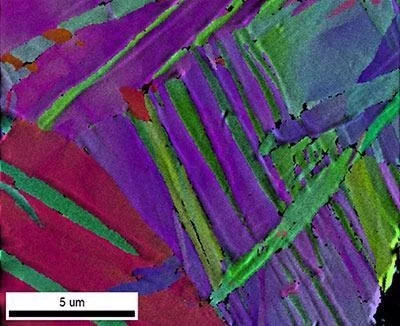
EBSD Image Quality and IPF orientation map from cryo-forged nanotwinned titanium collected at 7 kV and 200 pA beam dose for improved spatial resolution. Image Credit: Gatan
Traditional materials
- Extremely clear EBSD patterns can be gathered without the need for optical or phosphor lenses.
- Spatial resolution improves with lower acceleration voltages.
- High-dynamic-range imaging is employed to obtain high EBSD pattern quality.
Conclusion
The Clarity EBSD Detector Series ensures unmatched sensitivity and pattern quality when it comes to EBSD pattern collection and mapping. Users can use this system to investigate beam-sensitive materials and can obtain quantifiable data on electron intensities spanning the broadest range of beam energies.

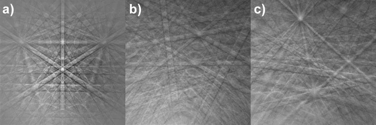
High-quality EBSD patterns collected with Clarity from a) silicon, b) olivine, and c) quartz. Image Credit: Gatan
