May 13 2009
As device performance requirements increase at the 3xnm technology node and beyond, the requirements for photoresist strip and clean are changing significantly. Shallower junctions and more abrupt gate electrode profiles are driving lower energy, higher dose implant steps, with doses typically in the 1E15cm-2 to 1E16cm-2 range. While these higher implant doses are necessary for improved device performance, they create challenges for photoresist removal such as the formation of thicker, cross-linked polymer "crusts" on the top surface layer of the resist.
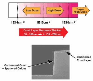 Photoresist "crust" caused by high dose implants
Rapid removal of this crust at higher temperatures can lead to resist "popping," a condition where solvents in the resist outgas through the crust and generate residues on the wafer surface, negatively impacting device yield. After the crust is removed, the bulk resist is stripped away, and any remaining residues are cleaned from the wafer surface. Use of a fluorine-based chemistry such as CF4 is the most efficient gas for this task; however, use of fluorine technology can be a challenge for some plasma-based systems requiring specific hardware modifications. In addition, the multiple temperatures and chemistries required for the High Dose Implant Strip (HDIS) process pose significant throughput challenges for strip systems based on single wafer process architectures.
Confronting the challenges of HDIS integration at the 3x/2xnm node, Novellus (NASDAQ: NVLS) has developed a residue-free strip process using CF4-based chemistries. The process runs on the GxT® photoresist strip platform that uses Novellus' multi-station sequential processing architecture (MSSP) to independently control chemistry and temperature at each process station. In the first step, the polymerized crust is removed, without popping, using an optimized process temperature. Subsequent stations, set to different temperatures, quickly remove the remaining resist and eliminate any residues from the wafer surface. No temperature or gas stabilization time is required between these steps, as would be required in a single wafer tool. MSSP enables the integration of optimized temperatures and chemistries for crust removal, bulk strip, and residue cleaning without sacrificing overall throughput. Figure 3 shows how residues are eliminated using Novellus' multi-temperature, CF4-based solution in comparison to non-CF4 approaches on the market. The GxT system has been engineered to be CF4-tolerant, resulting in world-class defectivity levels under high volume manufacturing conditions.
"Higher dose implants are creating significant photoresist removal challenges at the 3x/2x technology node," said David Cheung, director of technology for the Surface Integrity Group at Novellus. "Novellus' optimized CF4-based processes and MSSP architecture provide residue-free results, while providing industry-leading throughput for advanced HDIS applications."