Sep 29 2010
University of Michigan scientists using AFOSR-funding have created the smallest pixels available that will enable LED, projected and wearable displays to be more energy efficient with more light manipulation possible and all on a display that may eventually be as small as a postage stamp.
This latest nanostructuring technology for the Air Force developed by Dr. Jay Guo, associate professor in the Department of Electrical Engineering and Computer Science at the University of Michigan and his graduate student researchers, Ting Xu, Yi-Kuei Wu and collaborator Dr. Xiangang Luo includes a new color filter made of nano-thin sheets of metal-dielectric-metal stack, which have perfectly-shaped slits that act as resonators. They trap and transmit light and transform the pixels into effective color filtering elements.
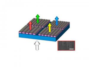 Color filters made of Plasmonic nano-resonators
The pixels created from this technology are ten times smaller than what are now on a computer monitor and eight times smaller than ones on a smart phone. They use existing light more effectively and make it unnecessary to use polarizing layers for liquid crystal displays (LCDs). They enable the backlighting on the LED to be used more efficiently. Prior to this technology, LCDs had two polarizing layers, a color filter sheet, two layers of electrode-laced glass and a liquid crystal layer, but only about five percent of the backlighting reached the viewer.
The research funded by AFOSR exploits nanophotonic devices using plasmonic structures.
"Most of the applications of the new technology suffer from the absorption loss by the presence of metal structure that is an integral part of the plasmonic devices," said Guo.
However, the loss in structure can be managed to produce useful devices that are valuable to the Air Force which is considering the technology to be used as part of virtual displays integrated to pilots' windshields.
In the near future, the scientists are expecting to use nanoimprint lithography to begin making the next generation of color filters.
"We hope to show that the fabrication of these structures can be scaled up to large areas and can be very cost effective," said Guo.
According to Dr. Gernot Pomrenke, the AFOSR program manager overseeing Guo's research, many defense and aerospace applications require unique imaging techniques and compact systems. He noted that over the last several years plasmonics has become a significant research area to explore new capabilities for such systems.
"This research group has been able to harness light more effectively through their approach and bring benefits to sensing application," Pomrenke said. "Prof. Guo has also been a leader in nanoimprint lithography to more rapidly create the smaller patterns and structures for more cost-effective system manufacturing and integration."
Source: http://www.wpafb.af.mil/