The Alphacen 300 Drive is a sophisticated atomic force microscopy (AFM) system designed for 300 mm wafer metrology. It uses a precise tip-scanning platform to provide stable, reproducible, and exceptionally low-noise measurements.
With WaveMode technology, the system delivers line rates up to 15× faster than conventional in-air AFM while maintaining tip sharpness – allowing fast, high-resolution analysis and consistent results to support strict quality control in demanding semiconductor environments.
- Ultra-stable stage design
- High reproducibility
- High throughput
- Low cost of ownership
The design of the Alphacen 300 Drive is optimized for analyzing intricate samples, providing minimal noise, maximum stability, and sub-micron positioning – ensuring uncompromised performance even on ultra-smooth surfaces, so every detail can be trusted.
Robust Surface Roughness Metrology
The Alphacen 300 Drive delivers high-precision, Angstrom-level surface roughness metrology with exceptional reproducibility. This performance is driven by a combination of advanced stage engineering and WaveMode, Nanosurf’s proprietary photothermal off-resonance imaging technology.
By maintaining consistently low, quantitative interaction forces between the tip and the sample, WaveMode preserves tip sharpness even during prolonged use. This reliability ensures a user-friendly experience while significantly reducing the total cost of ownership by extending component lifespan.
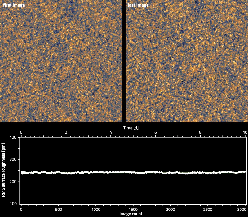
Time series of surface roughness measurements of a silicon wafer using WaveMode. Images in the top row show images at the beginning of the series and after 10 days. The graph below shows the roughness for each image in the series. Image Credit: Nanosurf AG
Ultra-Stable Stage Design
The Alphacen 300 Drive is engineered to deliver dependable measurements, even on ultra-smooth surfaces. Its ultra-stable stage offers low noise, high stability, and sub-micron positioning accuracy, supporting complex sample analysis.
Built on over two decades of expertise in industrial stage engineering, the system provides the rigidity and performance required for high-performance AFM metrology.
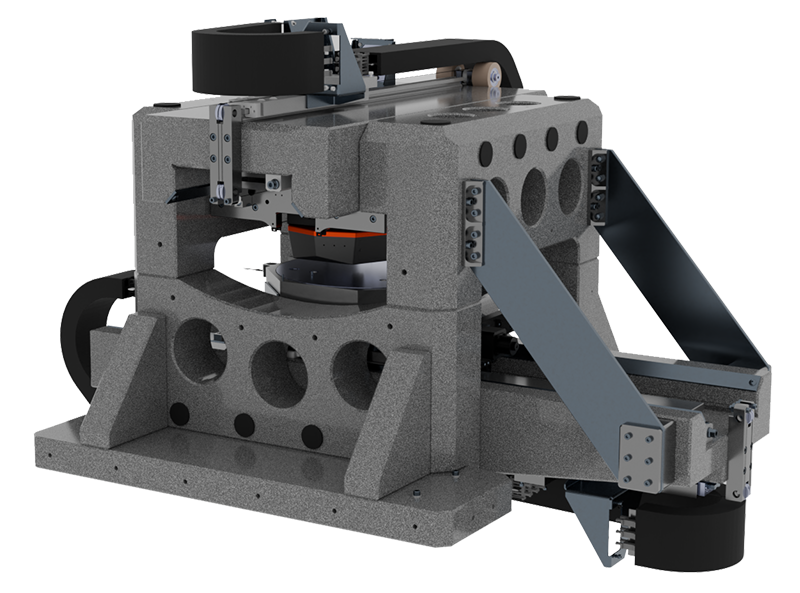
Image Credit: Nanosurf AG
Fastest Angstrom-Level Surface Roughness Metrology
WaveMode significantly accelerates surface roughness characterization while maintaining high precision, effectively bypassing the speed limitations of traditional in-air imaging techniques.
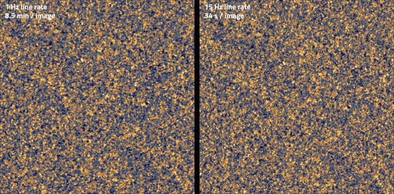
Comparison of silicon wafer surfaces acquired at the standard 1 Hz line rate and at the 15 Hz line rate achievable with the Alphacen 300 Drive. Image Credit: Nanosurf AG
Wafer Edge and Sidewall Inspection
The new wafer edge and sidewall inspection approach provides detailed characterization of wafer edges and sidewalls, extending from the top surface to the apex with sub-nanometer resolution.
High-resolution profiles and images reveal critical regions of the wafer that were previously difficult to observe, offering valuable insights into process control and optimization.
Nanosurf Studio: Just Press Play
The software developers and application specialists carefully evaluated the experience of performing atomic force microscopy (AFM) measurements to provide a solution that allows one to focus on their experiments and final results. Just Press Play.
- Personalize the software interface to accommodate both expert and novice users
- Intuitive system designed for new users with extensive flexibility for experienced users
- Take advantage of a fully automated AFM setup, including laser alignment, spring constant and sensitivity calibration, tip approach, and data acquisition
- Access advanced wafer automation capabilities, including automatic wafer alignment and KLARF file import
- Confidently navigate samples using integrated ViewPort optical sample navigation
- Take advantage of fully scriptable instrument control for custom automation and integration
Specifications
Source: Nanosurf AG
| . |
. |
| Scan head |
DriveAFM: High-resonance frequency flexure-guided scanner with direct drive actuation
100 µm x 100 µm x 20 µm range (XYZ) |
| Operating modes |
WaveMode, WaveMode-NMA, CleanDrive-based Dynamic and Phase imaging, Static Mode, Lateral Force Mode, Scanning Spreading Resistance Microscopy, Conductive AFM, Scanning Microwave Microscopy, Force Spectroscopy, I-V Spectroscopy, FastScanning Option, and many more |
| Stage |
XYZ range: 640 mm x 300 mm x 16 mm
Movement velocity: 100 mm/s
Encoder resolution: 10 nm
Repositioning accuracy (bidirectional): <500 nm |
| Sample Mount |
300 mm wafer chuck with integrated lift pins; compatible with 200 mm wafers |
On-axis
optics |
Top-view camera for simultaneous cantilever and sample observation
Field of view: 1100 µm x 850 µm
Camera resolution 2592 px x 1944 px, 15 fps @ full resolution |
Off-axis
optics |
Camera for wafer alignment
10x objective
Field of view: 900 µm x 700 µm |
| Acoustic isolation |
STC 34+ |
| Cleanroom rating |
ISO 5 |