In last week’s announcement of the Nobel Prize in Physics, the Royal Swedish Academy of Sciences lauded graphene’s “exceptional properties that originate from the remarkable world of quantum physics.” If it weren’t hot enough before, this atomically thin sheet of carbon is now officially in the global spotlight.
The promise of graphene lies in the simplicity of its structure—a ‘chicken wire’ lattice of carbon atoms just one layer thick. This sheet confines electrons in one dimension, forcing them to race across a plane. Such quantum confinement results in stellar electronic, mechanical and optical properties far beyond what silicon and other traditional semiconductor materials offer. What’s more, if graphene’s electrons were restricted in two dimensions, like in a nanoribbon, it could greatly benefit logic switching devices—the basis for computation units in today’s computer chips.
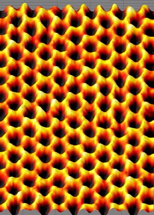 This image of a single suspended sheet of graphene taken with the TEAM 0.5, at Berkeley Lab’s National Center for Electron Microscopy shows individual carbon atoms (yellow) on the honeycomb lattice.
Now, Berkeley Labs materials scientist Yuegang Zhang and colleagues at University of California, Los Angeles are moving toward more efficient devices by studying the ‘noise’ in such graphene nanoribbons—one-dimensional strips of graphene with nanometer-scale widths.
“Atomically-thin graphene nanoribbons have provided an excellent platform for us to reveal the strong correlation between conductance fluctuation and the quantized electronic structures of quasi-one-dimensional systems,” says Zhang, a staff scientist in the Inorganic Nanostructures Facility at the Molecular Foundry. “This method should have much broader use to understand quantum transport phenomena in other nanoelectronic or molecular devices.”
Zhang and colleagues previously reported ways of fabricating films of graphene (http://newscenter.lbl.gov/feature-stories/2010/04/08/graphene-films/) and revealing low-frequency signal-to-noise ratios for graphene devices on a silica substrate (http://newscenter.lbl.gov/news-releases/2010/08/06/noise-in-graphene/). In the current study, the team made graphene nanoribbons using a nanowire mask-based fabrication technique. By measuring the conductance fluctuation, or ‘noise’ of electrons in graphene nanoribbons, the researchers directly probed the effect of quantum confinement in these structures. Their findings map the electronic band structure of these graphene nanoribbons using a robust electrical probing method. This method can be further applied to a wide array of nanoscale materials, including graphene-based electronic devices.
“It amazes us to observe such a clear correlation between the noise and the band structure of these graphene nanomaterials,” says lead author Guangyu Xu, a physicist at University of California, Los Angeles. “This work adds strong support to the quasi-one-dimensional subband formation in graphene nanoribbons, in which our method turns out to be much more robust than conductance measurement.”
A paper reporting this research titled, “Enhanced conductance fluctuation by quantum confinement effect in graphene nanoribbons,” appears in Nano Letters and is available to subscribers online . Co-authoring the paper with Zhang and Xu were Carlos Torres, Jr., Emil Song, Jianshi Tang, Jingwei Bai, Xiangfeng Duan and Kang L. Wang.
Portions of this work at the Molecular Foundry were supported by DOE’s Office of Science.