Scientists at Princeton have developed a sensor that helps track multiple substances from cancer to hidden explosives.
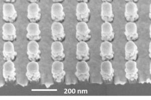 Princton's Micrograph of Sensor to Detect Eaman Scattering
The sensor has been fabricated to magnify faint signals emitted by laser light dispersion from a fabric kept on it. It allows multiple materials, each measuring as small as a nanoparticle, to be detected simultaneously depending on the color of the light they reflect.
Stephen Y. Chou, professor of electrical engineering who led the team, says they have developed a method to magnify the signals of the Raman sensor in an endeavor to change the concept of the use of Raman scattering. The enhanced signals were detected only at a few random sites on the sensor. This made it tough for the team to decide where to measure the signal, causing an overall weak signal. So they fabricated a new SERS design, a chip set with consistent arrays of nano-pillars constructed from metals and insulators.
The design consisted of a pit caused by metal on the top and bottom of each pillar and metal particles measuring 20nanometers in diameter, called plasmonic nanodots, placed on the wall of the pillar, with nano-spaces of two nanometers separating the metal particles. The nano-particles and gaps magnify the Raman signal. The holes act as antennae, using the laser light so that it passes the plasmonic nanodots numerous times to emit the Raman signal. The cavities also increase the Raman signal output. The sensor has been named the ‘disk-coupled dots-on-pillar antenna-array’ or D2PA. It is consistently sensitive, making it a dependable option for sensing devices.
The chip is cost- effective and can be developed in large quantities because it is easy-to-construct and combines two nanofabrication technologies, nanoimprint, a technique where nano-structures can be developed in a cookie-cutter manner, and self-assembly, a method where nano-particles form autonomously. The chips have been built on 4inch wafers and can increase the construction to a bigger wafer size.
Source: http://www.princeton.edu