A laser centre having a UV laser facility was recently launched in Thun by Empa director Gian-Luca Bona, and the Mayor of Thun, Raphael Lanz. The research facility will enable development of films with micro to nanometre accuracy.
 A team led by Paul Braun, professor of materials science and engineering at the University of Illinois at Urbana-Champaign has developed battery electrodes that are based on nanostructured metal foams in order to create a lithium-ion battery that takes two minutes to be 90% charged.
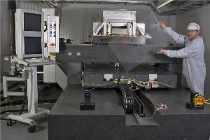
Crealas will operate the facility in collaboration with Empa. In the centre of the facility is a pulsed ultraviolet laser beam ablating nanometre-thin layers from large surfaces of three sqm. A granite table that weighs 19 tons was brought to the facility late last year and serves as the base.
Creating nanostructures on the surface leads to new physico-mechanical properties. They can minimize friction, lower drag or prevent fungal growth. Films used in optical structures that can control light can help develop three-dimensional screens that operate without glasses.
According to Patrik Hoffman, who heads the Advanced Materials Processing lab at Empa, the technology could help develop windowpanes, which would serve as solar panels during the day and illuminate interiors at night. He also hopes to develop materials that could be used to form electrical connections on flexible screens or solar cells.
The facility will help develop molding tools to mass manufacture structured films cost -effectively. It will also help develop optical security features such as optical three-dimensional effects.
Source: http://www.empa.org