May 18 2011
A recent study at the National Institute of Standards and Technology (NIST) may have revealed the optimal characteristics for a new type of computer memory now under development. The work, performed in collaboration with researchers from George Mason University (GMU), aims to optimize nanowire-based charge-trapping memory devices, potentially illuminating the path to creating portable computers and cell phones that can operate for days between charging sessions.
The nascent technology is based on silicon formed into tiny wires, approximately 20 nanometers in diameter. These "nanowires" form the basis of memory that is non-volatile, holding its contents even while the power is off-just like the flash memory in USB thumb drives and many mp3 players. Such nanowire devices are being studied extensively as the possible basis for next-generation computer memory because they hold the promise to store information faster and at lower voltage.
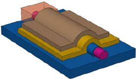
 In this schematic image, a silicon nanowire is shown surrounded by a stack of thin layers of material called dielectrics, which store electrical charge. NIST scientists determined the best arrangement for this dielectric stack for the optimal construction of silicon nanowire-based memory devices.
Credit: Schematic Zhu, GMU. TEM Bonevich, NIST.
Nanowire memory devices also hold an additional advantage over flash memory, which despite its uses is unsuitable for one of the most crucial memory banks in a computer: the local cache memory in the central processor.
"Cache memory stores the information a microprocessor is using for the task immediately at hand," says NIST physicist Curt Richter. "It has to operate very quickly, and flash memory just isn't fast enough. If we can find a fast, non-volatile form of memory to replace what chips currently use as cache memory, computing devices could gain even more freedom from power outlets - and we think we've found the best way to help silicon nanowires do the job."
While the research team is by no means the only lab group in the world working on nanowires, they took advantage of NIST's talents at measurement to determine the best way to design charge-trapping memory devices based on nanowires, which must be surrounded by thin layers of material called dielectrics that store electrical charge. By using a combination of software modeling and electrical device characterization, the NIST and GMU team explored a wide range of structures for the dielectrics. Based on the understanding they gained, Richter says, an optimal device can be designed.
"These findings create a platform for experimenters around the world to further investigate the nanowire-based approach to high-performance non-volatile memory," says Qiliang Li, assistant professor of Electrical and Computer Engineering at GMU. "We are optimistic that nanowire-based memory is now closer to real application."