Posted in | News | Graphene

New Scalable Fabrication Technique for Graphene Transistors

Researchers of the California Nanosystems Institute at UCLA along with researchers from UCLA Henry Samueli School of Engineering and Applied Science and UCLA Department of Chemistry and Biochemistry have developed a scalable technique for the damage-free fabrication of self-aligned graphene transistors.

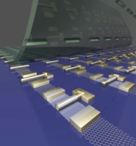
Self-alligning graphene transistors (Credit: UCLA)

Graphene is derived from graphite and is a single-layered structure of carbon atoms. Its properties make it an ideal candidate to operate as transistors to facilitate the development of smaller and faster electronic devices.

Large scale fabrication of graphene is impeded by the dwindling scale of electronic devices and graphene’s distinctive properties. When conventional fabrication techniques are employed for graphene manufacture, the performance and lattice shape of graphene often gets damaged in the process that leads to problems such as serial resistance and parasitic capacitance when employed in circuits. The new method involves the use of a sacrificial substrate for carrying out the lithography, deposition and etching steps and subsequent employment of a physical transferring process to integrate the pattern with graphene.

The method paves way for damage-free, self-aligned graphene transistors with a cutoff frequency of 400 MHz, the highest till date for graphene transistors. The results show the potential for graphene in ultra high frequency devices.

The research is funded by the National Institutes of Health, the National Science Foundation and the U.S. Office of Naval Research.

Source: http://www.ucla.edu

Will Soutter

Written by

Will Soutter

Will has a B.Sc. in Chemistry from the University of Durham, and a M.Sc. in Green Chemistry from the University of York. Naturally, Will is our resident Chemistry expert but, a love of science and the internet makes Will the all-rounder of the team. In his spare time Will likes to play the drums, cook and brew cider.

Citations

Please use one of the following formats to cite this article in your essay, paper or report:

  • APA

    University of California, Los Angeles. (2019, February 12). New Scalable Fabrication Technique for Graphene Transistors. AZoNano. Retrieved on April 19, 2024 from https://www.azonano.com/news.aspx?newsID=25190.

  • MLA

    University of California, Los Angeles. "New Scalable Fabrication Technique for Graphene Transistors". AZoNano. 19 April 2024. <https://www.azonano.com/news.aspx?newsID=25190>.

  • Chicago

    University of California, Los Angeles. "New Scalable Fabrication Technique for Graphene Transistors". AZoNano. https://www.azonano.com/news.aspx?newsID=25190. (accessed April 19, 2024).

  • Harvard

    University of California, Los Angeles. 2019. New Scalable Fabrication Technique for Graphene Transistors. AZoNano, viewed 19 April 2024, https://www.azonano.com/news.aspx?newsID=25190.

Tell Us What You Think

Do you have a review, update or anything you would like to add to this news story?

Leave your feedback
Your comment type
Submit

While we only use edited and approved content for Azthena answers, it may on occasions provide incorrect responses. Please confirm any data provided with the related suppliers or authors. We do not provide medical advice, if you search for medical information you must always consult a medical professional before acting on any information provided.

Your questions, but not your email details will be shared with OpenAI and retained for 30 days in accordance with their privacy principles.

Please do not ask questions that use sensitive or confidential information.

Read the full Terms & Conditions.