Advantest Corporation (TSE: 6857, NYSE: ATE) today announced that it has developed a new EB (electron beam) lithography system, the F7000, with superior resolution performance meeting the requirements for 1Xnm technology nodes. The F7000 supports substrates of diverse materials, sizes, and shapes, including nanoimprint templates as well as wafers, and is optimized for diverse applications such as advanced LSIs, photonics, MEMS, and other nano-processes.
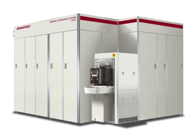 EB Lithography System F7000 (Photo: Business Wire)
The F7000 will be featured in Advantest’s exhibit (booth #3D-803 in Hall 3) at the SEMICON Japan trade show, December 5-7 in Makuhari Messe in the Chiba prefecture. The company plans to launch sales of the new system in the fiscal year ending March 2014.
A Flexible Next-Generation Lithography Solution
Competition in the mobile electronics and other categories has sparked an urgent need for chip-makers to develop increasingly low-power, highly functional semiconductors while reducing TTM (time to market). As a result, manufacturers are looking to EB lithography, which writes fine-pitch patterns directly onto wafers, as a method of accelerating cutting-edge semiconductor R&D processes. Advantest’s new F7000 offers the company’s proven EB technology in a system capable of writing patterns as fine as 1Xnm. The system also supports template fabrication for nanoimprint lithography—a technology positioned to take center stage in next-generation semiconductor manufacturing.
Product Features
1Xnm Resolution Performance
Advantest has developed a new column technology—key to electron beam writing accuracy—which delivers resolution performance meeting the needs of cutting-edge semiconductor R&D at the 1Xnm node.
Supports Substrates of Diverse Sizes, Shapes, & Materials
The F7000’s adjuster function enables it to write to diverse sizes of wafer, glass substrates, and also square substrates. Moreover, simply by switching adjusters, the system can support silicon, gallium arsenide, and substrates of other materials, utilizing separate adjusters for each material to avoid contamination.
“Lab to Fab” Flexible Configuration
Users can select the configuration optimal for their needs, either stand-alone or in-line, enabling the F7000 to support a wide array of applications from R&D to volume production.
High Throughput
With increased current density, the F7000 achieves a write speed fully 5 times faster than its predecessor model, the F3000.
Small Footprint
The F7000 features a footprint 40% smaller than that of the F3000.