As part of the FP7 NanoMend project, The Centre for Process Innovation (CPI), IBS Precision Engineering and The University of Huddersfield have been working together to design and manufacture a state-of-the-art Wavelength Scanning Interferometer system that enables the fast surface measurement of low contrast defects at pre-industrial scale.
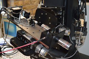 NanoMend Wavelength Scanning Interferometer
The tool will be installed at CPI’s National Printable Electronics Centre in June 2014. A demonstration video of the Wavelength Scanning Interferometer can be viewed here.
Current industry standard interferometry systems generally work by mechanically scanning the position of a lens relative to the substrate being measured. Such a technique is too slow to perform the large number of measurements required to enable defect detection analysis for large-scale ultra barrier films. The solution to this is to use wave length scanning, which is able to produce a quantitative measurement of the film layer topographies in the form of a three dimensional image. Analysis of thin film defects with interferometry can provide richer information on the nature of the defect, so its significance may be assessed.
The Wavelength Scanning Interferometer developed by the NanoMend consortium analyses defects by using 3D technology and is able to perform at the speed required for ultra barrier films at proof of concept scale.
The Wavelength Scanning Interferometer has been designed to make 3D measurements without mechanical movement of the optics, by varying the wavelength of the light source in an interferometer setup. The aim is to produce a full 3D measurement and analysis of a lateral stripe of the surface of a web in a matter of seconds. An assessment of a larger area of the web surface can be built up from a series of these stripes. The technique has been invented and proven at laboratory scale at The University of Huddersfield and the installation at CPI provides the infrastructure to scale up the technology to provide proof of concept data on roll-to-roll manufacturing processes for high performance ultra barrier. The Wavelength Scanning Interferometer instrument will be retrofitted to an existing web handling tool at CPI, with a technology roadmap devised to advance the development towards wider industrial applications in thin film quality assurance.
The NanoMend project is a pan-European collaborative, end user led project aimed at pioneering novel technologies for in-line detection, cleaning and repair of micro and nano scale defects on thin films deposited on large area substrates. The consortium includes a mix of industrial and academic partners and has received €7.25 Million of funding from the EU FP7 Programme.