ROHM has recently established a process for MEMS (Micro Electro Mechanical System) utilizing thin-film piezoelectric elements, and implemented the industry's first* foundry business that integrates product design and manufacturing processes, from wafer pulling to mounting, in order to meet a variety of customer needs.
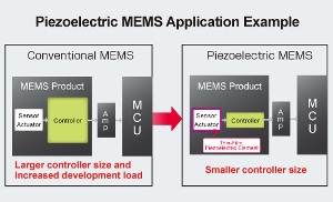
Piezoelectric elements, which possess the inherent property of generating a voltage when pressure is applied, are incorporated into a wide variety of electronic devices, from conventional inkjet printheads to autofocus systems in infrared and standard cameras. Combining these elements with MEMS technology, which is commonly used in accelerometers and gyroscopes, makes it possible to simplify design and reduce the size of processing controllers, contributing to increased performance, lower costs, and greater end-product miniaturization. In addition, the energy-saving characteristics of the piezoelectric element itself, which requires very little power during standby, are garnering increased attention – particularly in the sensor market where explosive growth is expected.
We have already begun conducting joint development of piezoelectric MEMS products based on customer requirements and gradually expanding our production lines to accommodate growth markets, such as industrial inkjet printers, sensors, and wearable devices. Going forward ROHM will continue to integrate piezoelectric elements with MEMS technology in order to achieve greater miniaturization and energy savings.
However, in the device creation of piezoelectric MEMS, thin-film deposition that possesses high piezoelectric properties and precision fabrication and molding of micro-piezoelectric elements are difficult to realize. Furthermore, high-precision processing is required for the MEMS drive block, and additional knowledge and expertise – along with the cultivation of new technologies – are needed in order to support next-generation applications and emerging markets.
In response to these challenges, ROHM is actively engaged in the research of thin-film piezoelectric elements. Based on the findings of Professor Isaku Kanno of the Graduate School of Engineering at Kobe University on evaluation measurement methods for thin-film piezoelectric elements, and by taking advantage of development synergy created by combining the collective production technologies of the entire ROHM Group, which includes ROHM's ferroelectric technology cultivated for long-term memory, LAPIS Semiconductor's high-sensitivity MEMS/mounting technology, and Kionix's MEMS miniaturization technology, we were able to establish a manufacturing process at LAPIS Semiconductor Miyazaki and provide piezoelectric MEMS optimized for a variety of markets and applications.
ROHM's MEMS processes utilizing thin-film piezo elements offer 5 key advantages:
- Integrated production system, from wafer pulling to mounting, enables complete control of product manufacturing for unsurpassed quality and flexibility
- 1500m2 clean room built for specifically for IC microfabrication
- 6-inch wafers utilized (8-inch wafers planned)
- Round-the-clock operation speeds up development while enabling early production startup
- Expanded production capacity (600K/M → 2000K/M)
Applications
- Accelerometers, gyroscopes, pressure sensors
- Inkjet printheads
- Infrared sensors and cameras
- Autofocus function in cameras
- Microphones and speakers
- Actuator/nozzle control
- Energy harvesting
Terminology
- Piezoelectric element
- A piezoelectric element converts force applied to the piezoelectric body into voltage, or it can refer to a passive device that utilizes the piezoelectric effect to convert voltage into power.
- Besides actuators and sensors, it is also used in filters and oscillators in analog electronic circuits. Source: http://www.rohm.com/
- MEMS (Micro Electro Mechanical Systems)
- Refers to devices that integrate a number of components, such as sensors, actuators, and mechanical parts (drive block) on a single substrate.
- In the semiconductor industry MEMS are typically used in accelerometers and gyroscopes, but are expected to play a major role in next-generation smartphones, IT equipment, and sensor networks that support smart communities of the future.