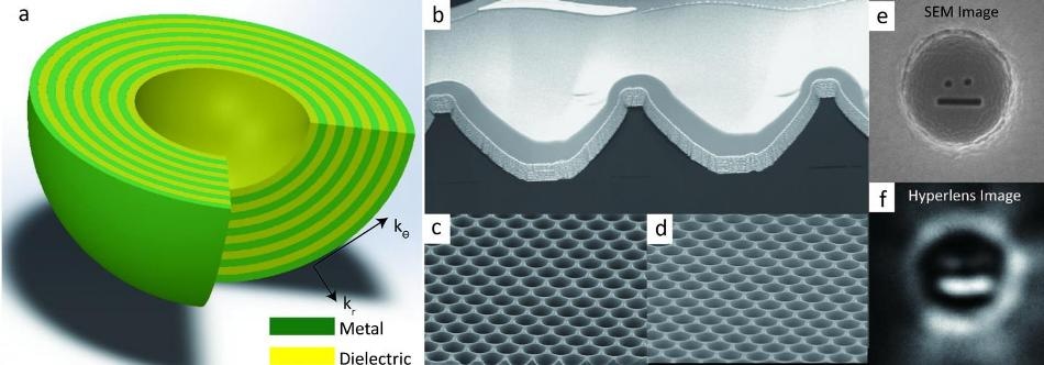
 a) This is a multilayered spherical hyperlens structure. Metal and dielectric thin films are deposited on a spherical shape of substrate. b) This is a transmission electron microscopy (TEM) image of the cross-section of a replicated hyperlens c & d) Tilted view for the quartz master mold and the replicated substrate e) Scanning electron microscopy (SEM) image of the sub-diffraction scale objects. f) Far-field optical image after hyperlens. The small object below diffraction limit is clearly resolved by the hyperlens. CREDIT: Image provided by POSTECH.
For many centuries, lens makers have worked hard to make a perfect lens with the ability to produce pristine and perfect images. In the year 1873, Ernst Abbe—a German physicist and optical scientist—found out the diffraction limit of the microscope.
Put differently, he found out that traditional lenses fundamentally cannot capture all the details of a given image. From that time, this field has seen innumerable developments in producing images of very higher resolution when compared to diffraction-limited optics.
In 2000, Professor Sir John B. Pendry from Imperial College London proposed a technique for producing a lens that has a theoretically perfect focus. John Pendry was the one who globally attracted millions of Harry Potter fans with the probability of making a real Invisibility Cloak. Diffraction restricts the maximum resolution of any optical imaging system. However, theoretically perfect lens proposed by Pendry will be fabricated using metamaterials to surpass the diffraction limit of traditional lenses, where metamaterials are materials engineered to exhibit characteristics that do not occur naturally. Going beyond this restriction in resolution in traditional optics can catapult optical imaging science and technology into domains dreamt by only common Muggles.
Internationally, researchers have attempted to accomplish super-resolution imaging that captures minute details in evanescent waves that might otherwise be lost while using traditional lenses. Hyperlenses are super-resolution tools with the ability to modify scattered evanescent waves into propagating waves, which helps in projecting the image into the far-field. Present-day studies dealing with a single hyperlens produced out of an anisotropic metamaterial that has a hyperbolic dispersion have exhibited real-time far-field sub-diffraction imaging. Yet, the drawback of such tools is that they have a very small observation area, as a result necessitating accurate positioning of the subject. Although a hyperlens array can be seen as a probable solution, such an array might be very challenging and excessively costly to produce by means of prevalent nanofabrication techniques.
A study by Professor Junsuk Rho’s and his colleagues from the Department of Mechanical Engineering and the Department of Chemical Engineering at Pohang University of Science and Technology in cooperation with researchers from Korea University has contributed at an exceptional level to overcome this challenge by indicating a reliable and scalable fabrication technique for large-scale production of a hyperlens device by means of direct pattern transfer methods. The study has been reported in the world-renowned journal Scientific Reports.
The researchers adopted nanoimprint lithography to overcome the main drawbacks of the earlier techniques used for fabricating hyperlens devices. They used a simple pattern transfer process to easily fabricate a perfect large-scale hyperlens device on a replicated hexagonal array of hemispherical substrate that has been directly pattern-transferred and printed from the master mold. The next process is to perform metal-dielectric multilayer deposition by means of electron beam evaporation. The hyperlens array, with dimensions of 5 cm x 5 cm is shown to resolve sub-diffraction characteristics as less as 160 nm under visible light with a wavelength of 410 nm.
Professor Rho believes that the innovative and cost-efficient fabrication technique discovered by the researchers can be adopted to fabricate multitudes of practical real-time, far-field super-resolution imaging devices with wide applications in nanotechnology, biology, medical science, optics, and other related interdisciplinary fields.