Dec 11 2017
Regardless of their size, the functioning of computers or mobile phones depends on the interaction among a wide range of materials. Hence, researchers and engineers ought to have an in-depth understanding of precisely the manner in which particular chemical elements in a transistor diode or a computer chip function, and also the consequences of bonding between these elements.
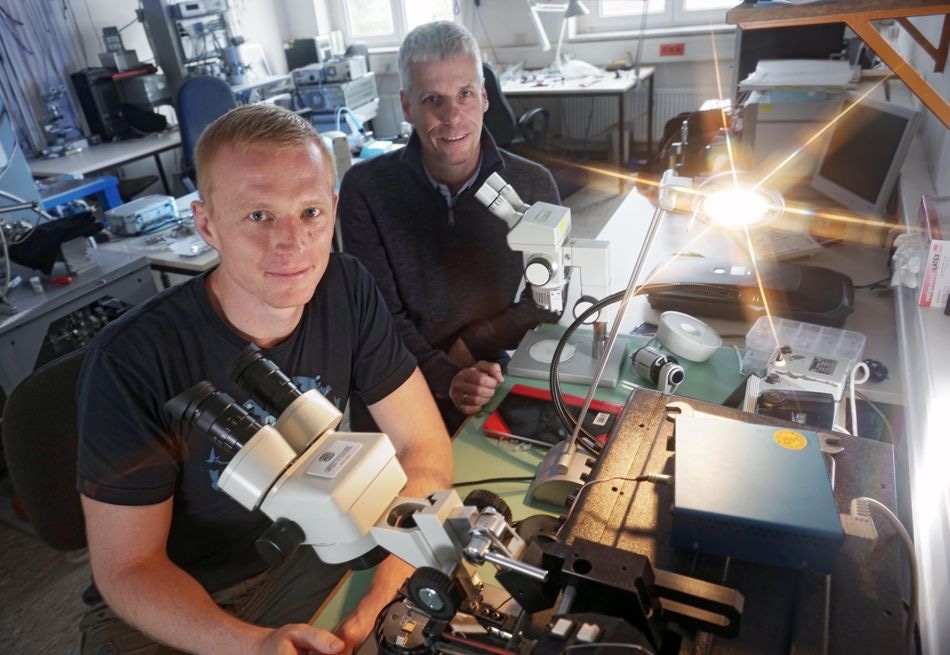 The physicists Andreas Johannes (l.) and Carsten Ronning in a laboratory at the Institute of Solid State Physics of Friedrich Schiller University Jena. CREDIT: Jan-Peter Kasper/FSU.
At present, a team of physicists from Friedrich Schiller University Jena, Germany, has devised a new technique that allows them to acquire various different kinds of information concurrently from the inner side of a nanoscale building block while the block is still in the active state. The physicists from Jena and their collaborators have published their outcomes in the latest issue of Science Advances, a specialist journal.
“Using our method, we can obtain information at one and the same time about the elements’ composition, that is to say the fraction between the elements; about their oxidation grade, which means their valence state or the nature of the bond; and finally about internal electrical fields that have thus been created,” stated Professor Dr Carsten Ronning from the University of Jena. “These are all elementary indicators for the component’s function,” added Ronning, who has led the study. Yet, in the process devised by the Jena physicists, with partnership from collaborators from Grenoble, Madrid, and Vienna, the components under study need not be prepared in detail or probably even disintegrated. “In principle, we can X-ray the diodes of a mobile phone while it is switched on, without damaging it,” stated Ronning.
X-ray beam from the particle accelerator
A conclusive aspect of the research strategy is a very precisely focused X-ray beam, using which the Jena team, at first, X-rayed a device specifically designed to carry out their experiments. “We introduced arsenic and gallium atoms into a silicon wire around 200 nanometres thick. When heated, these atoms agglomerate at one point, that is to say they mass together, which produces a functional component,” explained Professor Ronning. “We then ran a 50-nanometre-wide X-ray beam along the wire, thus irradiating it bit by bit.” The scientists showed that similar to a solar cell, the arrangement mixture of materials transformed the X-rays into electric current that flow in just one direction, similar to a diode. Through this strategy, the team rendered visible the intrinsic electrical fields indispensable for functioning of the component. Moreover, the component discharged light. “The X-rays excite the atoms in the building block, which emit a characteristic radiation,” elucidated Dr Andreas Johannes, who carried out the experiments. “In this way we obtain a spectrum, which gives us valuable information about the individual elements present and their relative ratios.” When the energy of the X-rays is changed, the well-known X-ray absorption spectra which allow the team to make affirmations on the oxidation grade of the elements, and also on the bonds themselves, are generated.
Obtain all these types of information through one measurement
“Now, it is possible to obtain all these types of information through one measurement by using our method,” stated Andreas Johannes. Despite the fact that comparable outcomes are probable by adopting electron microscopy, here, the devices ought to be specifically developed and probably disintegrated because the penetration depth of the electron beam is considerably more restricted. Furthermore, such evaluations can be carried out only in a vacuum, but the X-ray technique is practically does not depend on any particular environment.
To date, narrow X-ray beams such as these can be produced only by using particle accelerators, a reason for the Jena physicists to working in close collaboration with the European Synchrotron Radiation Facility (ESRF) in Grenoble, France, to devise the innovative measuring technique. These facilities are accessible not only to scientific researchers but also industry to X-ray prevalent components with higher accuracy and, most importantly, to attempt using new combinations of materials to develop components that function on par. “For example, our method can be of value in developing new batteries,” stated Andreas Johannes. “Because researchers would also like to examine these, especially while in use and fully operational, for example to determine the oxidation grades of the elements.”