Jun 20 2019
Physicists have discovered a unique type of nanotube that produces current when exposed to light. Devices such as infrared imaging chips and optical sensors are probable applications, which could be beneficial in fields such as astronomy and automated transport. In the future, if the effect can be magnified and the technology expanded, it could result in high-efficiency solar power devices.
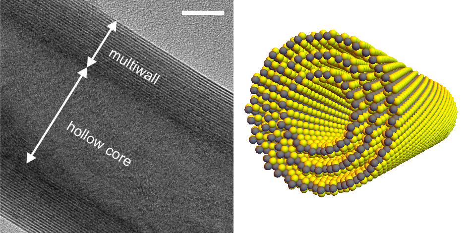 Transmission electron microscopy image of a hollow core nanotube. The white scale bar corresponds to 10 nm (left). Rendering of a nanotube (right). Image: © 2019 Iwasa et al.
Collaborating with an international team of physicists, University of Tokyo Professor Yoshihiro Iwasa was investigating probable functions of a special semiconductor nanotube when he had a lightbulb moment. He took this proverbial lightbulb (which really was a laser) and shone it on the nanotube to learn something informative. Some wavelengths and intensities of light triggered a current in the sample — this is referred to as the photovoltaic effect. There are numerous photovoltaic materials, but the behavior and nature of this nanotube is cause for interest.
Essentially our research material generates electricity like solar panels, but in a different way. Together with Dr. Yijin Zhang from the Max Planck Institute for Solid State Research in Germany, we demonstrated for the first time nanomaterials could overcome an obstacle that will soon limit current solar technology. For now, solar panels are as good as they can be, but our technology could improve upon that.
Yoshihiro Iwasa, Professor and Physicist, University of Tokyo
The current-inducing nanotube is composed of rolled-up sheets of a special semiconductor material based on tungsten disulfide (WS2). The sheets do not trigger a current when exposed to light except if rolled into tubes. This is an emergent behavior, one not natural to the material until it is altered. What is exciting is how it varies from current photovoltaic materials.
Normally, photovoltaic solar panels utilize a specific arrangement of materials called a p-n junction. This is where two different types of materials (p-type and n-type) are attached, which on their own do not produce a current in the presence of light, but when placed together. P-n junction-based photovoltaics have developed in efficiency over the last eight decades or so since their finding. However, they are getting near their theoretical boundaries due in part to their necessity for the arrangement of numerous materials.
WS2 nanotubes do not depend on a junction between materials to obtain the photovoltaic effect. When in the presence of light, they produce a current throughout their whole structure or bulk. This is known as the bulk photovoltaic effect (BPVE) and it happens as the WS2 nanotube is not symmetrical if one was to reverse it. If it were symmetrical, the current triggered would not have a preferred direction and therefore would not flow. So other symmetrical nanotubes — such as the well-known carbon nanotubes — do not display BPVE despite being robust electrical conductors.
Our research shows an entire order of magnitude improvement in efficiency of BPVE compared to its presence in other materials. But despite this huge gain, our WS2 nanotube cannot yet compare to the generating potential of p-n junction materials. This is because the device is nanoscopic and will be difficult to make larger. But it is possible and I hope chemists are inspired to take on that challenge.
Yoshihiro Iwasa, Professor and Physicist, University of Tokyo
In the long run, scientists expect that this kind of material could enable fabrication of more efficient solar panels. But given the predictable size restrictions in the near term, it is more probable to find use in other applications. BVPE could be used to develop more sensitive and higher-fidelity infrared or optical sensors. These have further applications in sensor-laden self-driving cars, embedded monitoring devices, or even in the imaging sensors for astronomical telescopes.
“My colleagues from around the world and I eagerly explore the potential of this unprecedented technology,” concluded Iwasa. “For me, the idea of creating new materials beyond anything nature could provide is a fascinating reward in its own right.”