Understanding and managing charge carrier quasiparticle movement in atomically thin 2D materials is critical for effective nano-excitonic systems.
According to new research, the drift-dominant exciton diverting into the flexure local area allows the scientists to precisely restrict excited states of 2D dichalcogenides at the nanometer scale.
Utilizing spectroscopic tip-enhanced luminescence spectroscopy with less than 15 nm magnification, the researchers study the spatio-spectral features of routed excitons in WSe2 monolayers and transformed trions in MoS2 monolayers.
Gigapascal-scale point pressure optimization also controls exciton diverting and trion exchange rate. A drift-diffusion process confirms an exciton diverting effectiveness of 25% with a strain rate (0.1%), above prior research’s effectiveness of 3%. This study allows effective exciton transit and trion transformation in 2D semiconductor materials.
Benefits and Limitations of Thin Semiconductors
Atomically thin semiconductors outperform similar low-dimensional semiconductors like quantum dots and nanorods in 2D exciton dispersing. This fascinating characteristic has implications in optoelectronics as well as photovoltaics; however, regulating exciton dynamics is difficult for quantum computation processors and exciton-integrated electronics.
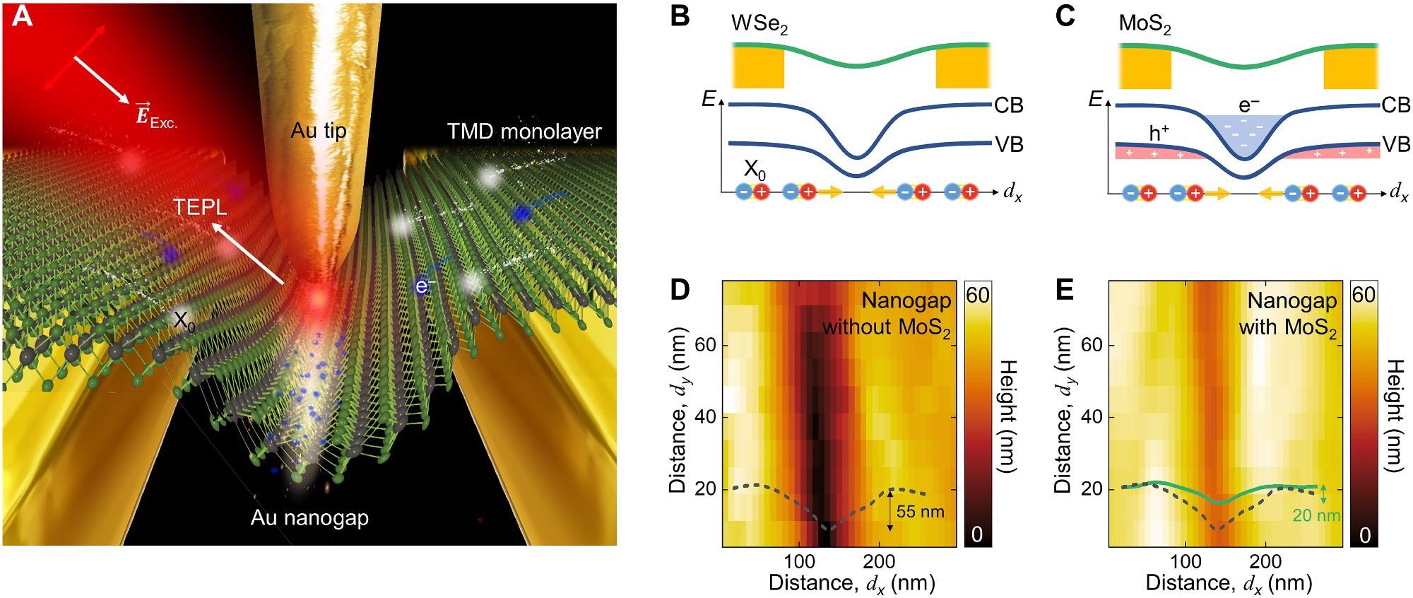
Figure 1. Schematic illustrations of an experimental design and energy diagram. (A) The Au nanogap device and transferred TMD MLs combined with TEPL spectroscopy to probe and control the electric charges (e−) and exciton (X0) dynamics at the nanoscale. Illustrations of the energy band diagram for WSe2 (B) and MoS2. CB, conduction band; VB, valence band. (C) MLs on the nanogap and spatial distributions of electric charges (e− and h+) and photoexcited excitons (X0). AFM topography images and height profiles of the nanogap without (D) and with (E) MoS2 ML exhibiting a wrinkled crystal structure, which gives rise to a nanoscale strain gradient. © Lee, H. et al., (2022).
Strategies to Modify the Exciton Behavior of 2D TMDs
Various strain engineering techniques have recently been proved to be effective in manipulating the exciton behavior of 2D transition metal dichalcogenides (TMDs), including drift-induced excitonic fluctuation and diffusion-induced energy transfer.
Because of their atomic thickness, 2D materials can drastically alter their electronic structures and excitonic capabilities by modulating the crystallographic strain in the material.
To accomplish stochastic exciton funneling to a narrow bandgap area, several researchers have sought to fabricate strain-gradient equipment, such as wrinkled surfaces, mechanical transducers, and atomic force microscopy (AFM) tips.
However, recent research has shown that at ambient temperature, the exciton funneling effectiveness adopting these methodologies is considerably lower due to strong dispersion in the microscale bandgap-gradient zones, which overwhelms the essential drift mechanism.
Because the drift mechanism, unlike the arbitrary diffusion process, has orientation in the bandgap-gradient zone, increasing the concentration of the drift-dominant zone is a critical component in achieving high funneling efficiency.
![Hyperspectral TEPL imaging of strained TMD MLs at the wrinkle. TEPL spectra of WSe2 (A) and MoS2 (B) MLs at the crystal face (green) and the wrinkle (red) regions. (C to F) Hyperspectral TEPL images of a WSe2 ML. AFM topography image with a description of exciton funneling (C). TEPL images of the spectrally integrated intensity of excitons (D) [spectral region of IX0 in (A)] and low-energy shoulder (E) [spectral region of IX- in (A) after normalization]. TEPL image of spectral linewidth (F). (G to J) Hyperspectral TEPL images of a MoS2 ML. AFM topography image with a description of electron funneling and trion (X-) conversion (G). TEPL images of the spectrally integrated intensity of excitons (H) [spectral region of IX0 in (B)] and low-energy shoulder (I) [spectral region of IX- in (B) after normalization]. TEPL image of spectral linewidth (J). a.u., arbitrary units.](https://www.azonano.com/images/news/ImageForNews_38664_16444863280514444.jpg)
Figure 2. Hyperspectral TEPL imaging of strained TMD MLs at the wrinkle. TEPL spectra of WSe2 (A) and MoS2 (B) MLs at the crystal face (green) and the wrinkle (red) regions. (C to F) Hyperspectral TEPL images of a WSe2 ML. AFM topography image with a description of exciton funneling (C). TEPL images of the spectrally integrated intensity of excitons (D) [spectral region of IX0 in (A)] and low-energy shoulder (E) [spectral region of IX- in (A) after normalization]. TEPL image of spectral linewidth (F). (G to J) Hyperspectral TEPL images of a MoS2 ML. AFM topography image with a description of electron funneling and trion (X-) conversion (G). TEPL images of the spectrally integrated intensity of excitons (H) [spectral region of IX0 in (B)] and low-energy shoulder (I) [spectral region of IX- in (B) after normalization]. TEPL image of spectral linewidth (J). a.u., arbitrary units. © Lee, H. et al., (2022).
Ideal TMD Device
Until recently, the majority of investigations created a significant amount of strain on the crystal, resulting in a decrease in crystal quality and photonic quantum efficiency.
Because of this, it is extremely desirable to develop an optimal TMD device, with a higher exciton funneling efficiency, substantial quantum efficiency, and minimal induced strain.
Furthermore, to increase the connectivity of quantum devices and exciton-integrated electronics, the exciton funneling route must be dramatically shrunk down from its present microscale sizes to nanoscale dimensions.
Trion Transformation at the Funneling Region
Another fascinating finding from the previous work was the transformation of trions in a WS2 monolayer's funneling area.
They discovered that free electrons are effectively routed towards the area with the smallest bandgap and linked to neutralized excitons to generate the trion configuration with almost 100% energy conversion even at room temperature.
With the capacity to regulate the behavior of excitons and trions, this unique trait significantly expands the array of uses for 2D excitonic systems.
However, since the prior study focused only on exciton funneling and trion transformation in n-type TMD monolayers using optical aberrations spectroscopy, it created a misunderstanding about the impact of doping variants and the area of the bandgap-gradient zone.
Thus, elevated spatio-spectral research of distinct TMD MLs in conjunction with a linked characterization of their morphological, photonic, and computational features is critical for a thorough understanding of exciton dynamics at their characteristic size range.
The researchers in this study demonstrated the use of a nanogap device to support reduced and extremely efficient exciton funneling and trion conversion operations at ambient temperature.
![Hyperspectral TEPL imaging of TMD MLs at the nanogap. TEPL spectra of WSe2 (A) and MoS2 (B) MLs at the Au surface (green) and the nanogap (red) regions. (C to F) Hyperspectral TEPL images of a WSe2 ML. AFM topography image with a description of exciton funneling (C). TEPL images of the spectrally integrated intensity of excitons (D) [spectral region of IX0 in (A)] and low-energy shoulder (E) [spectral region of IX- in (A) after normalization]. TEPL image of spectral linewidth (F). (G to J) Hyperspectral TEPL images of a MoS2 ML. AFM topography image with a description of electron funneling and trion (X-) conversion (G). TEPL images of the spectrally integrated intensity of excitons (H) [spectral region of IX0 in (B)] and low-energy shoulder (I) [spectral region of IX- in (B) after normalization]. TEPL image of spectral linewidth (J).](https://www.azonano.com/images/news/ImageForNews_38664_16444863345446529.jpg)
Figure 3. Hyperspectral TEPL imaging of TMD MLs at the nanogap. TEPL spectra of WSe2 (A) and MoS2 (B) MLs at the Au surface (green) and the nanogap (red) regions. (C to F) Hyperspectral TEPL images of a WSe2 ML. AFM topography image with a description of exciton funneling (C). TEPL images of the spectrally integrated intensity of excitons (D) [spectral region of IX0 in (A)] and low-energy shoulder (E) [spectral region of IX- in (A) after normalization]. TEPL image of spectral linewidth (F). (G to J) Hyperspectral TEPL images of a MoS2 ML. AFM topography image with a description of electron funneling and trion (X-) conversion (G). TEPL images of the spectrally integrated intensity of excitons (H) [spectral region of IX0 in (B)] and low-energy shoulder (I) [spectral region of IX- in (B) after normalization]. TEPL image of spectral linewidth (J). © Lee, H. et al., (2022).
Research Findings and Conclusion
Using TEPL spectrometry on a nanogap device, this work showed low-threshold exciton transit and dynamic control.
The researchers discovered that 0.1% strain at the nanogap enhanced TEPL amplitude by 180%, equal to the strain gradient induced by 10% strain at the microscopic scale.
This technique reduces the tension required to identify observable exciton funneling. This was attributed to the nanoscale strain gradient's high funneling efficiency, which enabled it to occupy more than 60% of the drift-dominant region. Additionally, the Au tip's precise spatial position and gigapascal-scale pressure enable reversible regulation of exciton behavior in WSe2 and MoS2.
The ability to manipulate exciton dynamics spatially on the nanoscale is critical for future exciton-based photonics breakthroughs.
As a result, the scientists suggested their method will allow higher quantum yield and more connectivity in next-generation exciton-based optoelectronic devices.
Reference
Lee, H. et al., (2022). Drift-dominant exciton funneling and Trion conversion in 2D semiconductors on the nanogap. Science Advances, 8(5). Available at: https://www.science.org/doi/10.1126/sciadv.abm5236
Disclaimer: The views expressed here are those of the author expressed in their private capacity and do not necessarily represent the views of AZoM.com Limited T/A AZoNetwork the owner and operator of this website. This disclaimer forms part of the Terms and conditions of use of this website.