Image Credit: Ruijuan Tian, Xuetao Gan, Chen Li, Xiaoqing Chen, Siqi Hu, Linpeng Gu, Dries Van Thourhout, Andres Castellanos-Gomez, Zhipei Sun, Jianlin Zhao.
In the “post-Moore age,” this is critical for fostering the advancements in microelectronics technology, quantum information technology, and micro sensing technology.
Information technology has supported the development of photonic integrated chips or PICs. Silicon PICs, for example, are compatible with mature CMOS technology for low-cost and large-scale production. Silicon nitride PIC can tolerate moderately high optical power and significant fabrication errors.
Lithium niobate PIC can achieve perfect electro-optic modulations with low driven voltage and high linearity.
Moreover, the monolithic integration of waveguides and photodetectors with a single material is one of the disadvantages of modern PICs. The PIC materials cannot absorb the optical signal to maintain light transmission in the waveguide, making an integrated photodetector out of a single material unachievable.
On PICs, hetero-integrations of absorptive bulk materials (such as Ge, III–V compound semiconductors, and others) have been used to tackle this problem. The high prices, intricate manufacturing procedures, and material interaction concerns remain significant challenges.
Two-dimensional (2D) materials have recently gained popularity as photon-absorption materials for chip-integrated photodetectors. The lattice-mismatch limitations to hetero-integrate 2D materials with PICs are eliminated since there are no surface dangling bonds.
Semi-metallic graphene, insulating boron nitride, semiconducting transition metal dichalcogenides, and black phosphorus are 2D materials with a wide range of electrical and optical characteristics. As a result, chip-integrated photodetectors with varied spectral ranges could be built by selecting suitable 2D materials.
A research group led by Professor Xuetao Gan from the Ministry of Industry and Information Technology’s Key Laboratory of Light Field Manipulation and Information Acquisition and Shaanxi Key Laboratory of Optical Information Technology, School of Physical Science and Technology, Northwestern Polytechnical University, China, has reported that integrating van der Waals PN heterojunctions of 2D materials on optical waveguides can help realize chip-integrated photodetectors with low dark current, fast speed, and high responsivity.
Researchers can stack 2D materials with various qualities by “stacking wood” to build van der Waals heterostructures with atomically flat surfaces thanks to the 2D layered structure and no dangling connections.
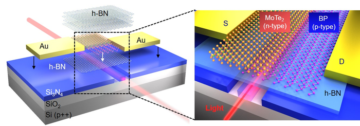
As demonstrated in the figure, the “arbitrary combination” of van der Waals heterojunctions can supply the advantages of a single material and develop fresh features, attaining a jump of 1+1>2. The researchers successfully manufactured van der Waals PN heterojunction using natural p-doped BP and n-doped MoTe2 for hetero-stacking in this study.
The second figure shows that, unlike conventional semiconductors, 2D materials do not require consideration of lattice mismatch when integrating with various photonic integration platforms since there are no dangling connections on the surface. Finally, source-drain electrodes can be created on the photonic platform using “stacking wood” technology and put on both sides of the material, eliminating time-consuming methods such as photolithography.
It also considerably simplifies the device’s manufacturing procedure and lowers the fabrication cost. It also evades the device interface contamination in processes such as photolithography, which considerably increases the device’s performance.
Journal Reference:
Tian, R., et al. (2022) Chip-integrated van der Waals PN heterojunction photodetector with low dark current and high responsivity. Light Sci Appl doi:10.1038/s41377-022-00784-x.