Stacking two comparable semiconductor monolayers with a twist angle induces novel physical phenomena, including moiré excitons and associated electronic phases, due to the formation of a moiré superlattice owing to modulations in periodic interlayer coupling. Hence, it is necessary to explore the underlying coupling mechanism between atomic levels to understand these novel phenomena.
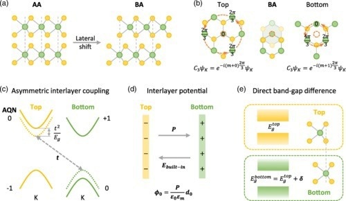
Figure 1. Schematic of asymmetric interlayer coupling in the 3R−MoS2 bilayer. (a) Side view of atomic structures of the 3R−MoS2 bilayer with AA (left) and BA (right) stacking configurations, where the yellow and green spheres denote the S and Mo atoms, respectively. (b) Schematic of the phase winding at K points in monolayer MoS2 when the C3 rotational center is located at a Mo site (left) and the hollow center of the hexagon formed by Mo and S (right). The middle is the top view of the atomic structure of the 3R−MoS2 bilayer with BA stacking configuration. The small, dashed orange circle denotes the C3 rotational center. (c) Electronic band structure at K points of a 3R−MoS2 bilayer with BA stacking configuration. Yellow (green) dashed lines denote the original uncoupled bands. Yellow (green) solid lines denote the bands of the top (bottom) MoS2 layer. Numbers denote the overall azimuthal quantum number (AQN) of the conduction or valence band edge at K points. Interlayer coupling t exists only between the conduction band of the top layer and the valence band of the bottom layer, resulting in a level repulsion t2/Eg between these two bands, where Eg is the direct band gap of MoS2. (d) Schematic of spontaneous out-of-plane polarization P pointing from the top layer (yellow) to the bottom layer (green) in a 3R−MoS2 bilayer with BA stacking configuration. (e) Schematic of direct band gap at the K point of the top (yellow) and bottom (green) layer in a 3R−MoS2 bilayer with BA stacking configuration. The atomic structure shows the nonequivalent environments of the Mo atom in the top and bottom MoS2 layers.
A study published in Physical Review X presented the interlayer coupling between the valence and conduction bands of two different layers. Its underlying mechanism was determined based on layer-dependent Berry phase winding. Studying the 3 rhombohedral (R)−molybdenum disulfide (MoS2) bilayer via optical spectroscopy in a dual-gated device revealed type-II band alignment at the K points.
Furthermore, the spontaneous polarization and underlying asymmetric interlayer coupling in 3R−MoS2 were determined quantitatively by unveiling their contributions to the band offset. This study sheds light on the physical basis of stacking-induced ferroelectricity of transition metal dichalcogenide (TMD) homostructures, which plays a crucial role in 2D semiconductor moiré physics.
Interlayer Coupling in TMDs
TMDs are 2D semiconductor materials with unique electrical, mechanical, and optical properties. The mixing and matching of monolayers of 2D materials offer a productive platform for exploring new quantum phenomena in vdW material-based systems.
When 2D materials are stacked individually, a lattice mismatch or twist angle may occur between the layers. Irrespective of their occurrence (naturally or by design), a moiré superlattice emerges, which is an interference pattern in atomic lattice structures.
Interlayer coupling is commonly found in vdW materials, offering the flexibility to modulate the electronic band structures of 2D materials. Adjusting the layer orientation of an artificial 2D assembly can bring about periodically tuned interlayer coupling in the moiré superlattice, leading to the emergence of exotic phenomena which are different from their monolayer counterparts.
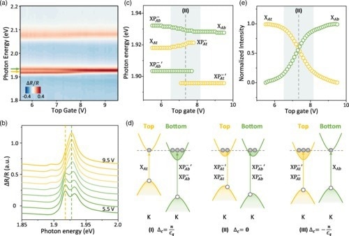
Figure 2. Electric-field-dependent reflectance contrast spectrum of intralayer excitons in 3R−MoS2 bilayer at a fixed electron doping density. (a) Contour plot of the electric-field-dependent reflectance contrast spectrum of 3R−MoS2 bilayer at a fixed electron doping density. The yellow and green arrows denote the intralayer A exciton, XAt and XAb, from the top and bottom layers, respectively. (b) Reflectance contrast spectrum at different top gate voltages in steps of 0.5 V. The bottom gate voltage is Vb=−0.85Vt+1.65. The yellow and green dashed lines denote XAt and XAb from the top and bottom layers, respectively. (c) From low energy to high energy, electric-field dependence of XP−'At (attractive exciton polaron in the top layer), XP−'Ab (attractive exciton polaron in the bottom layer), XAt or XP−At (intralayer exciton or repulsive exciton polaron, respectively, in the top layer), and XAb or XP−Ab (intralayer exciton or repulsive exciton polaron, respectively, in the bottom layer) energies extracted from (a). (d) Schematics of band alignment and existing optical transitions of a BA-stacked 3R−MoS2 bilayer at a fixed electron doping density when (I) the Fermi level reaches the conduction band edge of the top layer with Δc=n/Cq, (II) the Fermi level is in the conduction band of both layers and electrons are equally doped into two layers with Δc=0, and (III) the Fermi level is at the conduction band edge of the bottom layer with Δc=−n/Cq. (e) Normalized intensity changes of XAt and XAb extracted from (a) along the fixed photon energy indicated by yellow and green arrows. The crossing point denotes the same oscillator strength of XP−At and XP−Ab when the conduction band offset is zero as shown in the middle panel of (d).
In TMD 2D semiconductors, the moiré potentials quench the electron’s kinetic energy and localize them at the moiré superlattice’s energy local minimum, generating a new platform for simulating various correlated physics and creating quantum emitter arrays.
Monolayer MoS2 crystals have low state densities, which may limit their practical applications. MoS2 bilayer crystals are particularly attractive for applications in logic devices and sensors because of their high density of states, carrier mobility, and stability at room temperature.
Interlayer Coupling in Rhombohedral Stacked MoS2 Bilayer
A rhombohedral crystal structure of a TMD (with a parallelly oriented stack of TMD layers) was recently discovered with tunable spontaneous electric polarization, despite the absence of polarization in each layer.
This novel phenomenon transforms rhombohedral TMDs into ferroelectric semiconductors with the ability to absorb visible light, increasing their potential applicability in various devices. However, the mechanism underlying this phenomenon remains unclear.
In this study, an optical approach was adopted to examine the spontaneous polarization generated by the asymmetric interlayer coupling, which enables tuning of the characteristics of vdW materials owing to its dramatic changes at different twist angles of adjacent layers.
The research team focused on interlayer coupling, examining it via field-dependent optical spectroscopy in a dual-gated device based on homogeneous rhombohedral MoS2 bilayer. Here, the interlayer potential was compared with the energy difference between the conduction band edges in different layers.
The results revealed that coupling occurs only between the conduction band in one-layer and the valence band in another layer, but not vice versa. This interaction was termed asymmetric interlayer coupling.
In contrast to the graphene electrical sensing approach, the optical technique presented in this work does not rely on polarization switching via interlayer sliding, making it ideal for measuring spontaneous polarization in different materials.
The strength of the asymmetric interlayer coupling at K sites was quantified using optically measured band gaps and band offsets, which is critical for optoelectronic and ferroelectric applications of semiconducting TMDs with sliding ferroelectricity.
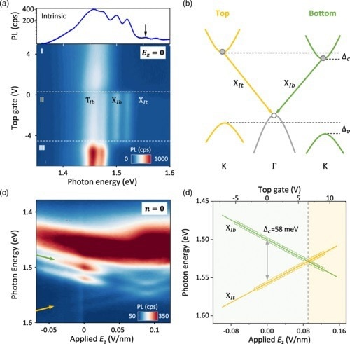
Figure 3. Doping-dependent and electric-field-dependent photoluminescence spectrum of Γ−K interlayer excitons in the 3R−MoS2 bilayer. (a) Contour plot of the doping-dependent PL spectrum of momentum-indirect interlayer excitons in the 3R−MoS2 bilayer without an external electric field. The gate voltage is applied proportionally on top and bottom gates with relation Vb=0.85Vt. At zero doping, from low energy to high energy, three pairs of peaks indicate TIb (interlayer trion), XIb (interlayer Γ−K exciton), and XIt (interlayer Γ−K exciton), respectively; XIt is more evident in (c) as indicated by the yellow arrow. The top is an average PL spectrum in region II with the black arrow denoting the XIt (interlayer Γ−K exciton). cps: counts per second. (b) Type-II band alignment of BA-stacked MoS2 bilayer at K points of the Brillouin zone and momentum-indirect Γ−K transitions. Δc and Δv denote the conduction band offset and valence band offset at K points, respectively. (c) Contour plot of the electric-field-dependent PL spectrum in the 3R−MoS2 bilayer with zero doping. The green (yellow) arrow denotes the interlayer exciton XIb (XIt). The gate voltage is applied proportionally on top and bottom gates with relation Vb=−0.85Vt. (d) Electric-field dependence of interlayer excitons extracted from (c). Solid lines denote the linear fitting results. The dashed gray line denotes the same energy of XIb and XIt when Δc=0.
Conclusion
In conclusion, the unique sensitivity of the Fermi polaron to charges doped at multiple levels was leveraged to investigate the inherent interlayer potential and, hence, the spontaneous polarization in a homogeneous 3R-MoS2 bilayer.
The research findings offered a solid framework for comprehending the moiré superlattices generated by twisted homostructures. In addition to the novel physics discovered by position-dependent interlayer coupling, the inter-layer hopping determined the moiré potential depth and bandwidth of moiré bands.
The competition between inter-layer hopping and Coulomb interaction has resulted in different correlated insulating states observed in various experiments. Thus, a thorough understanding of the interlayer coupling of different stacking orders is critical for investigating these novel semiconducting moiré materials.
Asymmetric coupling with additional unique functions can be achieved in the future by using heterostructures of various TMDs. Because polarization switching is not required, the present approach of optically investigating spontaneous polarization may be used for a wide range of polar semiconductors.
Reference
Liang, J., Yang, D., Wu, J., Dadap, J. I., Watanabe, K., Taniguchi, T., Ye, Z. (2022). Optically Probing the Asymmetric Interlayer Coupling in Rhombohedral-Stacked MoS2 Bilayer. Physical Review X. https://journals.aps.org/prx/abstract/10.1103/PhysRevX.12.041005
Further Reading
Nature Nanotechnology. (2022) Making a case for moiré semiconductors. [online] https://doi.org/10.1038/s41565-022-01184-3
Disclaimer: The views expressed here are those of the author expressed in their private capacity and do not necessarily represent the views of AZoM.com Limited T/A AZoNetwork the owner and operator of this website. This disclaimer forms part of the Terms and conditions of use of this website.