The Rise of Tandem Solar Cells with Perovskite
It is critical to improve the power conversion efficiencies of photovoltaic cells to expand their applications. Every solar cell is ultimately constrained by the substance it is built of, which impacts the efficiency it can reach.
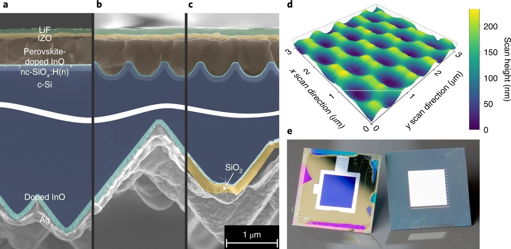
Figure 1. Nanotextured PSTSC design. a–c, SEM cross-section micrographs of the front and rear side of planar (a), nanotextured (b) and nanotextured + RDBL (c) PSTSCs. c-Si, crystalline silicon. d, AFM image of the nanostructured silicon bottom cell front side prior to the deposition of the contact layers. e, Photographs of the final PSTSC with a blue active area in between the front-side silver ring of approximately 1 cm2 (left) and the RDBL on the rear side (right). Image Credit: Stannowski, B., Becker, C. et al., Nature Nanotechnology
Monolithic dual-terminal perovskite-on-silicon tandem solar cells (PSTSCs) have recently managed to overcome the physiological limitation of traditional crystalline-silicon single-junction photovoltaic cells by achieving a PCE of greater than 31%.
Enhancements in the electronic and optical characteristics of perovskite-on-silicon tandem solar cells have allowed the PSTSCs to reach such high power conversion efficiencies.
The cell's polarity may be changed for better top-contact transmission as well as adjustment of the different layers for improved optical characteristics.
The electronic characteristics may be improved via optimization of the contact layers by using additives and altering the perovskite deposition.
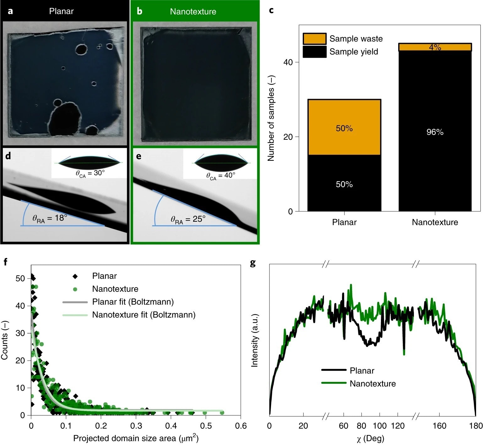
Figure 2. Perovskite film formation and morphology. a,b, Representative spin-coated perovskite films on planar (a) and nanotextured (b) silicon bottom cells covered by Me-4PACz (approximate area, 25 × 25 mm2). c, Fabrication yield of PCTSCs processed on planar and nanotextured silicon bottom cells. d,e, Side-view photographs of perovskite solution droplets on planar (d) and nanotextured (e) silicon substrate with roll-off angle (RA) and static contact angle (CA; inset) indicated. f, Projected area of domain sizes of perovskite layers deposited on planar and nanotextured substrates as determined from top-view SEM images (Supplementary Fig. 2). g, Azimuthal (χ) intensity profiles of the (100) reflection of perovskite averaged over 39 incidence angles from 0.1° to 2° as determined from GIWAXS measurements. Image Credit: Stannowski, B., Becker, C. et al., Nature Nanotechnology
How Can Texturing Improve Performance?
Effective light control plays an important role by providing nanostructured device interfaces for better power conversion efficiencies, as evidenced by numerical analyses of perovskite-on-silicon tandem solar cells.
For light control in Si-based photovoltaic cells, KOH-etched random pyramid textures with micrometer scale sizes are routinely utilized.
Unfortunately, these textures are incompatible with the solution-processed perovskite absorbers that have shown the greatest PCEs to date among all perovskite single-junction photovoltaic cells.
Different techniques for implementing light control textures in nanostructured PSTSCs have been examined thus far, either by altering the perovskite deposition method while keeping the pyramid texture unaltered or by modifying the pyramidal textures in a way that would make perovskite solution processing possible.
Developing a suitable texture capable of balancing the constant trade-off between optical and electronic capabilities of nanostructured PSTSCs having solution-processed perovskite top cells continues to prove challenging.
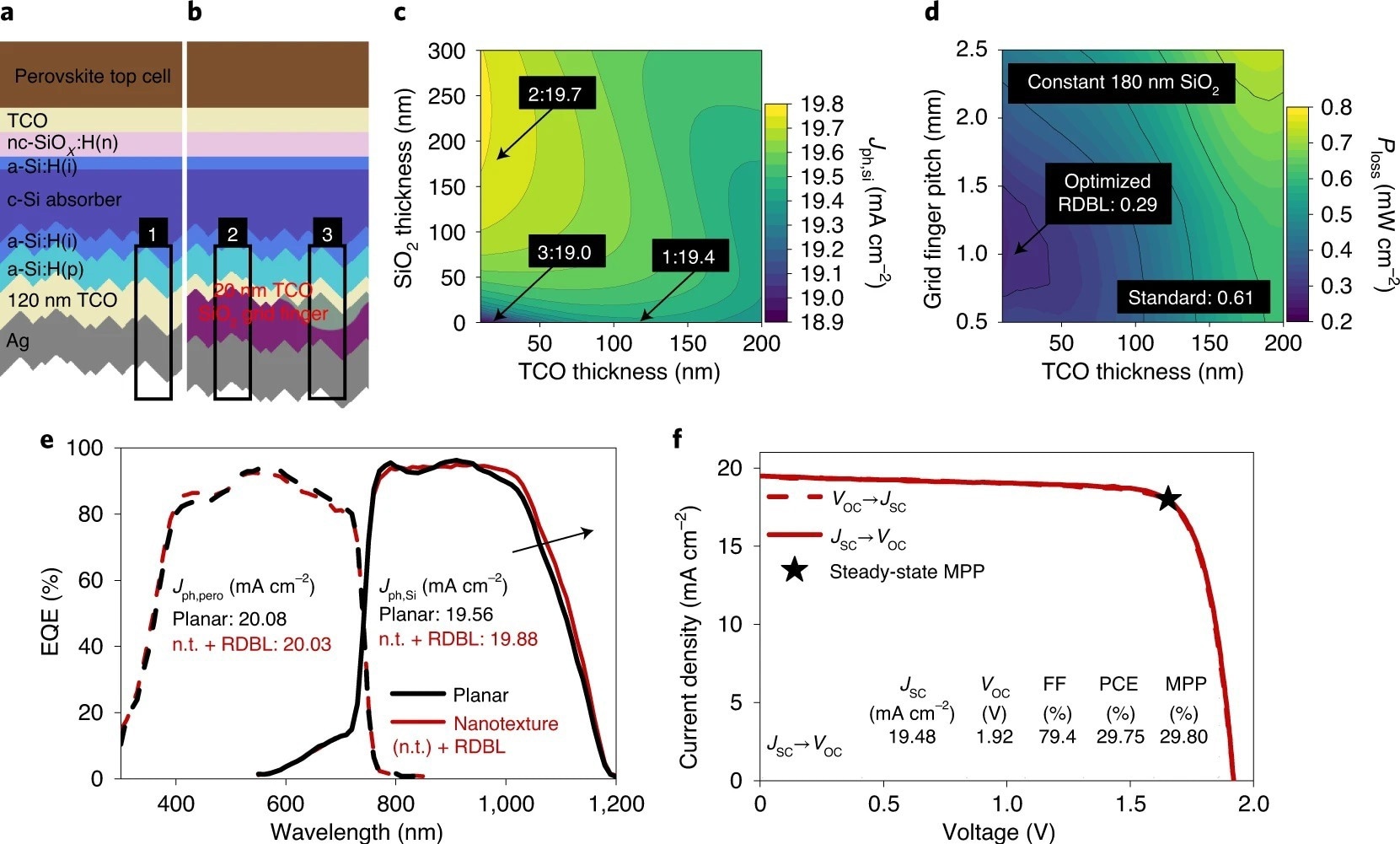
Figure 3. Implementing a rear RDBL for high-perfomance nanotextured PSTSCs. a,b, Schematic of the PSTSC layer stack with standard reflector (a) and with an RDBL at the rear side (b). (i), (n) and (p) refer to intrinsic, n-doped and p-doped layers. The numbered black frames mark the standard rear side (1) and the SiO2 (2) and grid finger (3) regions of the RDBL. c, 2D map of Jph,Si for different SiO2 (y axis) and TCO thicknesses (x axis). The configurations corresponding to the experimental layer stacks are marked with arrows and the corresponding Jph,Si is indicated. d, 2D map of power losses in the silicon bottom cell for different grid finger pitches (y axis) with 40 µm finger width and TCO thickness (x axis). Power loss in mW cm−2 is shown for the RDBL configuration and for the standard reflector. e, EQE spectra (dashed lines, perovskite EQE; solid lines, silicon EQE) of a planar PSTSC with a standard rear side (black) and a nanotextured (n.t.) PSTSC with an RDBL (red). The integrated photogenerated current densities of perovskite (Jph,pero) and silicon (Jph,Si) are shown. f, Current-density/voltage (J–V) characteristics of a nanotextured PSTSC with an RDBL certified by CalLab at Fraunhofer ISE. Image Credit: Stannowski, B., Becker, C. et al., Nature Nanotechnology
Highlights of the Research
Nanotexturing significantly reduces reflection losses, significantly boosts fabrication yield thanks to remarkable film-forming capabilities, and enhances open-circuit voltage by about 15 mV.
To mitigate parasitic absorption losses at near-infrared wavelengths, a reflector containing a dielectric buffer layer (RDBL) was added on the rear of the nanostructured silicon bottom cell.
The team, led by Dr. Bernd Stannowski, developed a perovskite-on-silicon tandem solar cell having a gentle sinusoidal nanotexture that added the benefits of the nanostructured silicon surface while retaining the material qualities of the solution-processed perovskite.
The group designed a nanostructured perovskite-on-silicon tandem solar cell with a gently grooved texture on the surface of the silicon bottom cell.
Commenting on the effect of the nanostructure, one of the authors, Dr. Christiane Becker said, “Most surprising, this texture brings several advantages at once: it reduces reflection losses and ensures a more regular perovskite film formation.”
Findings of the Study
In this work, the research team added gentle nanotexturing and an enhanced back-reflector arrangement into monolithic nanostructured PSTSCs.
The nanoscale textures allowed a significant increase in the process yield of perovskite top cells from about 50% for planar cells to almost 95% for nanostructured Si bottom cells.
A clear decrease in reflection losses was seen, amounting to a current density equivalent of about 0.5 mA cm-2. Total short-circuit current densities up to 40 mA cm-2 were detected in the silicon and perovskite cells.
Sensitivity studies revealed that the nanoscale textures significantly increased performance durability when there was a divergence from the ideal nanocrystalline SiO2 layer thickness.
A 15 mV rise in open-circuit voltage was a major driver for the enhanced PSTSC effectiveness. The increased open-circuit voltage resulted primarily from better perovskite cell performance, as evidenced by the subcell-selective electroluminescent characterizations.
Along with the nanoscale textures on the front of the Si bottom-cell, the team also integrated a reflector containing a dielectric buffer layer on the back.
By decreasing parasitic absorption losses, the perovskite-on-silicon tandem solar cell design enhanced the current density in the Si cell by about 0.3 mA cm-2.
Dr. Stannowski’s team achieved a certified power conversion efficiency of 29.8% by integrating RDBL and nanotextures in a single PSTSC. They argued that tailored nanotextures could assist in enhancing perovskite semiconducting materials on a number of levels.
The findings of this work are crucial for tandem perovskite-on-silicon solar cells, as well as for optoelectronic systems based on metal halide perovskites.
Reference
Stannowski, B., Becker, C. et al. (2022). Nano-optical designs for high-efficiency monolithic perovskite–silicon tandem solar cells. Nature Nanotechnology. Available at: https://doi.org/10.1038/s41565-022-01228-8
Disclaimer: The views expressed here are those of the author expressed in their private capacity and do not necessarily represent the views of AZoM.com Limited T/A AZoNetwork the owner and operator of this website. This disclaimer forms part of the Terms and conditions of use of this website.