Two-dimensional (2D) semiconductors made of materials such as transition metal dichalcogenides (TMDs) are forming the future of electronic devices. For these applications, 2D semiconductors provide the electronic and photonic properties that are of significant importance in determining the performance capability of certain transistors and lasers1, which are two of the many electronic products currently utilizing this technology.
To create such devices, a 2D sheet is formed onto a substrate through several different mechanisms including the exfoliation of flakes from a layered bulk source, as well as atomic layer and chemical vapor deposition.
While these techniques are adequate for small-scale production needs, large-scale high quality production of these 2D sheets has proven to be a major challenge for researchers and electronics developers.
With an average temperature requirement of above 550°C to deposit the material onto the substrate, a process that requires many hours to conduct, cost and practicality of the production of these devices are also important parameters to consider.
These limiting factors, in conjunction with a need in increasing the processing power of 2D conductors, have brought researchers to look towards enhanced techniques that are capable of producing multilayered, incredibly thin and flexible electronic wafers1.
Until now, no current technologies have been capable of creating atomically thin semiconductors with a large surface area; factors that play a significant role in determining the power potential of the device.
The research team of Dr. Kourosh Kalantar-zadeh at the School of Engineering at RMIT University in Melbourne, Australia2 have developed and tested a novel technique in response to the dynamic challenges present during the production of 2D semiconductors.
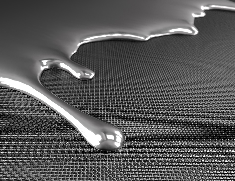
By manipulating liquid gallium (Ga), a post-transition metal with a low melting point of 29.8 °C, and placing this material onto a silicon dioxide (SiO2)-coated substrate, a 2D gallium oxide layer forms. Ga is an ideal material for this procedure as its low bulk viscosity when present as a liquid flows with impressive ease, a property that is much different than that of mercury. Liquid Ga also exhibits a low toxicity and virtually no vapor pressure when present at room temperature.
The significance of the gallium oxide layer that forms onto the SiO2 surface originates with a thickness of one-unit cell, in which the robust metal properties are stabilized at room temperature, preventing any possible deformations of the metal from occurring.
This surface oxide layer is also capable of strongly adhering to many materials, particularly oxides, through the weak Van der Waals forces dispersed across the surface1. Once liquid Ga is placed onto the substrate, it can be removed easily due to the low binding energy present on the surface oxide, which allows researchers to selectively pattern the deposited material on a wide range of surfaces such as glass and polymers.
The gallium oxide layer present on the patterned substrate is then sulfurized through a relatively low temperature (300 °C) two-step process, an applied heat that remains compatible with existing electronic device processing standards used today1. The low temperatures used in this process ensure uniformity among the constructed large area GaS bilayers, in which a relative thickness of 1.5 nm was found on the surfaces of the oxide-coated substrates.
The development of this printing method is not only compatible with the already established processes used in industry today, but it also offers an etchless patterning and deposition procedure that provides devices with a magnified performance capacity1.
Not only can the establishment of a gallium oxide layer allow for a new paradigm to be used for future electronics, optics, optoelectronics, sensors and other devices, but a large number of different metals can be alloyed from gallium to print both pure and mixed 2D oxides. This relatively simplistic, low temperature and cost-effective process allows industries to have a unique control over the surfaces of 2D semiconductors3.
References
- Carey, Benjamin J., Jian Zhen Ou, Rhiannon M. Clark, Kyle J. Berean, Ali Zavabeti, Anthony S. R. Chesman, Salvy P. Russo, Desmond W. M. Lau, Zai-Quan Xu, Qiaoliang Bao, Omid Kevehei, Brant C. Gibson, Michael D. Dickey, Richard B. Kaner, Torben Daeneke, and Kourosh Kalantar-Zadeh. "Wafer-scale Two-dimensional Semiconductors from Printed Oxide Skin of Liquid Metals." Nature Communications 8 (2017): 14482. Web.
- "Liquid Metal Nano Printing Set to Revolutionize Electronics." Phys.org. 17 February 2017. Web. https://phys.org/news/2017-02-liquid-metal-nano-revolutionize-electronics.html.
- "Liquid Metal Nano Printing Set to Revolutionise Electronics." RMIT University. 20 February 2017. Web. https://www.rmit.edu.au/
- Image Credit: Shutterstock.com/GraphicProcessor
Disclaimer: The views expressed here are those of the author expressed in their private capacity and do not necessarily represent the views of AZoM.com Limited T/A AZoNetwork the owner and operator of this website. This disclaimer forms part of the Terms and conditions of use of this website.