raigvi / Shutterstock
Naturally occurring in the form of sand or quartz, silicon is a readily-abundant material and a classic semiconductor.
Use of Silicon in Semiconductor Manufacturing
The use of silicon to make semiconductors for electronics calls for an ultrapure single crystal form. In this form, silicon atoms are regularly arranged into a crystal lattice with no undefined impurities present.
In addition to the single crystal form of silicon, there are also the polysilicon and amorphous silicon forms. While single crystal silicon used for microelectronics, the polycrystalline silicon, comprised of numerous ("poly") irregularly arranged single crystals, is useful for some electronics applications. Amorphous silicon is not used in the production of semiconductor electronics.
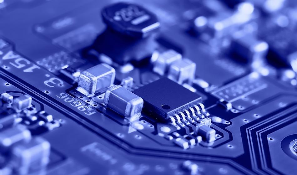
Silicon Wafers
The history of semiconductors in electronics is one of constantly shrinking circuits. A transistor is the basic unit of a circuit that drives every type of electronic gadget. As transistors have reduced in size, they have also become faster and required less electricity to function. For the past 40 years or so, shrinking transistor size has driven Moore’s Law, the rule of thumb that says electronic devices will double in speed and ability every 24 months. More specifically, Moore’s Law states the number of transistors that can fit on a chip will more or less double every two years.
The history of semiconductors has also coincided with the expansion of wafer size. Silicon wafers are thin slices of semiconductor used to create integrated circuits, which hold large numbers of transistors.
During the 1960s, a monocrystalline silicon wafer was around 20 mm across. Now, wafers 150 to 300 mm in diameter are standard. With larger wafers the throughput rate rises considerably in the production of microchips, resulting in decreased costs. As a result, with the exact same structure sizes, at least twice as many circuits can be generated on a 300 mm wafer as on a 200 mm wafer.
Transistor in Semiconductor Industry
One of the primary questions facing the 21st century semiconductor industry is: How small can a transistor be? Currently, businesses like Intel are producing silicon (which has an atomic size of about 0.2 nanometres) transistors 14 nanometres in diameter.
Subsequent generations of integrated circuits have had increasingly reduced power usage and faster processing speeds by reducing the processing unit and circuit size, and thus loading more transistors on a chip. The minimum unit size of the first-generation integrated circuit was 10 µm. This became smaller and smaller, ultimately reaching a point where the unit “µm” became cumbersome and was replaced by nm, with 1 nm equal to 1000 µm.
Over time, the lowest unit size has diminished at a rate of around 0.7 times per process node, from 90 nm to 45 nm to 20 nm. Today, we use a 16/14 nm node. Curiously, however, the minimum processing size of integrated circuits in the 14 nm node is considerably shorter than 14 nm.
The standard idea of a process node, where the actual processing takes place, is starting to lose its meaning. Today’s transistors are about 70 silicon atoms wide, so the potential for making them smaller is shrinking. Engineers are approaching the limit of how small a transistor can be, and while they do see ways to generate 3 and 2 nm semiconductors, commercial viability may end at 5 nm.
Three-Dimensional Transistors
Promising new technologies use a number of silicon layers to create three-dimensional structures of greater circuit density. This new structure can lower performance deviation by mitigating what's known as the "short-channel effect."
This emerging technology uses a gate to surround the channel on several sides and stop the leakage of electrons and holes. The usage of a three-dimensional structure also has the added benefit of making transistors smaller.
Sources
Disclaimer: The views expressed here are those of the author expressed in their private capacity and do not necessarily represent the views of AZoM.com Limited T/A AZoNetwork the owner and operator of this website. This disclaimer forms part of the Terms and conditions of use of this website.