Anucha Cheechang / Shutterstock
Atomic force microscopy (AFM) has become a powerful technique across many sectors and is a way of providing an accurate map of a surface’s topography and properties at the atomic level. Its suitability has grown across many sectors in the last few decades, and none more so than in the nanotechnology sector, where it has become a staple technique for nanomaterial analysis.
There are many techniques that are used to analyze nanomaterials, but those which are viable are those which can provide measurements at nanoscale dimensions and for microscopy techniques, the viable techniques are those which can provide a nanoscale resolution. Because AFM analyzes the surface atom by atom, it has an atomic resolution which is highly advantageous for analyzing both nanomaterials and the surface (at the nanoscale) of bulkier materials. Out of the many techniques, AFM has become one of the most suitable for analyzing nanomaterials and it is now one of the most widely used techniques as well.
What is AFM?
AFM is a specialist way of imaging a surface and varies in its operation compared to other microscopy methods. There are many different AFM imaging modes. Some modes will just image the relative positions of the atoms on the surface of a material, whereas other imaging modes will provide information on both the properties and the topography of the surface. In the cases where the properties are determined, most imaging modes will scan for the topography first, followed by a second scan to determine the properties. Each of these scans produces a visual map of the surface, and they can be superimposed to highlight the different atomic regions with their specific properties (e.g. conductive and insulating regions).
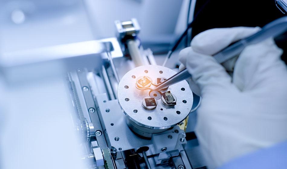
In terms of the operational principles, AFM uses a probe—composed of a piezoelectric cantilever and an atomically sharp tip—to scan the surface of a material. When the tip scans the surface, the intermolecular attraction between the tip and the surface pulls the tip towards the surface. In some modes, the tip touches the surface, but in non-contact mode, the tip moves towards the surface without touching it (the latter is used for softer materials, but as most nanomaterials are hard, the tapping mode is most common).
During the scan, a laser is directed on to the back of the cantilever arm. So, whenever the cantilever moves towards the surface, the laser beam is deflected relative to the position of the atom and the degree of deflection. This is recorded on a position-sensitive photodiode (PSPD). This occurs for each atom throughout the scan and each time the cantilever is deflected, it is reset back to its starting position by a feedback loop.
AFM and Nanomaterials
AFM is highly suitable for nanomaterial analyses, as it can be used to analyze all nanomaterials, as well as many aspects where nanomaterials are used. As well as the topography of the surface, the many different imaging modes available mean that the various properties of nanomaterials—or a nanoscale surface—can be determined, including the mechanical, electric, dielectric, optical and thermal properties of the surface. In many analyses of bulkier materials, the information obtained may only be true for the surface of the material—especially if it’s an active surface, as the properties may not be the same throughout the whole material. But nanomaterials have inherent thinness which means that the properties shown by the surface—which is an active surface in many cases—are often true for the whole nanomaterial. This becomes even more certain when 2D materials are being analyzed, as the materials being analyzed in these scenarios are essentially a single active surface (if it is a single layer 2D material).
Outside of the fundamental properties of nanomaterial, AFM can be used to probe the properties of materials and devices that use nanomaterials. One good example of this is nanoelectronic devices and components. AFM can be used to deduce the properties of the device and the fundamental properties of the active materials within a device. These range from mapping any piezoelectric and ferromagnetic domains, to the localized dielectric properties, and to see if the device is likely to experience any current leakage or electrical failure. These are just a few examples, but understanding the nanoscale properties of both nanoelectronic and conventional electronic devices is crucial for understanding how safe and efficient the device will be.
AFM can also be used alongside various nanofabrication methods to manipulate the structure and properties of various nanomaterials and to help to build new topological features on the surface of nanomaterials. These approaches can take the form of chemically modifying the surface of a nanomaterial with the AFM tip itself, or by using AFM alongside electron beam lithography and dip-pen lithography to physically remove atoms from the nanomaterial. In addition to changing the properties of the surface, these approaches can be used to produce a specific pattern on the surface of the nanomaterial. AFM can also be used to measure the effects that the manipulation approaches induce on the nanomaterial.
Sources
Disclaimer: The views expressed here are those of the author expressed in their private capacity and do not necessarily represent the views of AZoM.com Limited T/A AZoNetwork the owner and operator of this website. This disclaimer forms part of the Terms and conditions of use of this website.