There has been much research on the fabrication of nanochannels using local oxidation and consequent etching of silicon surfaces. Although this technique has been extensively demonstrated, it has the potential to obstruct the material removal process by generating a deposit over the etched area.
Image Credit: Foto-Ruhrgebiet/Shutterstock.com
Direct etching can be achieved without using any extra procedures if the oxide layer is removed by utilizing the tip alone. Previous research employed a catalytically active platinum-coated atomic force microscope (AFM) probe for material removal and displayed a direct etching approach over silicon without the development of oxide.
Aside from that, techniques like ion-beam sculpting, which uses low- and high-energy ion beams to create structures on the atomic scale, are useful.
Material removal on an atomic scale could result from a mix of actions like shearing and extrusion. Due to the compression of the substrate atoms by the tool edge atoms during the shearing process, the substrate atoms are forced upwards, generating the chips. On the other side, extrusion causes plastic deformation below the machined surface, and only a few chips are generated as a result of the extrusion process.
Since silicon is so widely used in the semiconductor sector, it should be subjected to more accurate and realistic material removal. Aside from that, silicon in the (100) orientation is preferable for structure construction research because the Si/SiO2 state density is lower than in the other orientation, resulting in higher carrier mobility when employed for nanodevice fabrications.
The research gap here is the minimal depth or height of atomic patterns that can be generated by employing AFM-based electrochemical and mechanical scratching procedures with an AFM tip to realize structure manufacturing.
Apart from Si, materials including highly oriented pyrolytic graphite (HOPG), gold, silicon carbide, and van der Waals materials like transition metal dichalcogenides (TMD) could be used in atomic-scale manufacturing experiments. As a first step, researchers demonstrated that a single atomic layer removal across HOPG may be done in the newly published study.
A comprehensive examination of oxide production on a silicon surface with platinum-coated while scratching when given a tip bias and material removal using a diamond tip, employing AFM, is presented in research published in the MDPI journal micromachines.
Methodology
Commercially accessible AFM equipment is used to execute the electrochemical etching technique. Including both contact mode for machining and amplitude modulation for imaging, a silicon-based AFM probe equipped with conductive PtIr5 and single-crystal diamond probes is used.
The schematic representation of an AFM-based electrochemical etching apparatus with a relative humidity control environment can be found in Figure 1.
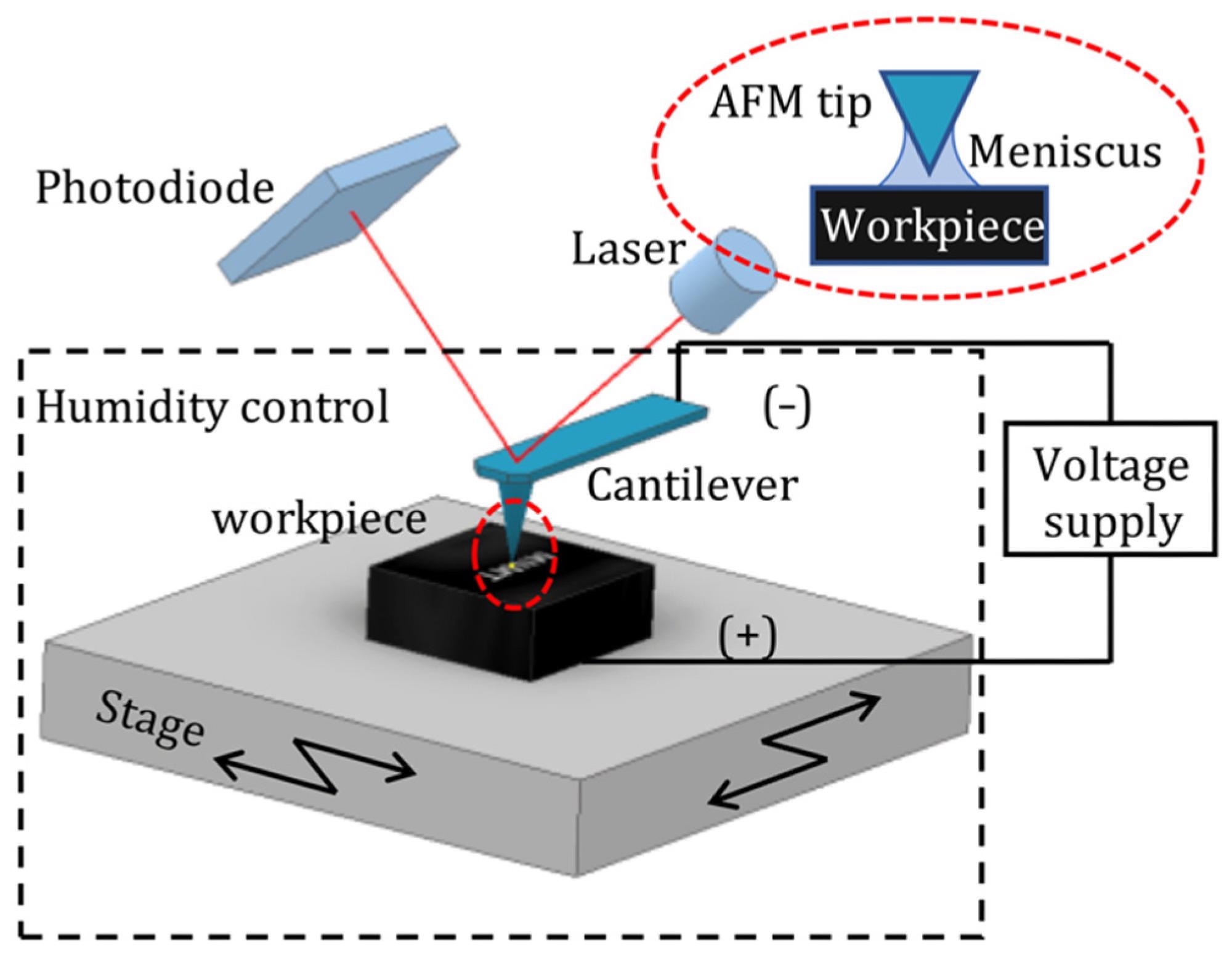
Figure 1. Schematic diagram of AFM-based electrochemical etching apparatus with a relative humidity control environment. Image Credit: Mathew, et al., 2022
Results and Discussion
In the presence of oxygen, the production of oxidation on the silicon substrate is well-known. In interaction with the adsorbed water layer on the silicon surface, the tip generates a water meniscus. Many parameters, like tip velocity, applied voltage, humidity, and applied tip force, can be used to influence the oxide deposition.
The oxide layer typically has a thickness of 1.5 to 2 nanometers. Local anodic oxidation (LAO) occurred when lines were scratched across the bare silicon substrate in normal room circumstances with a humidity of 36%. The lines were drawn with a force of 0.1 μN. This force is the smallest that can be applied to a silicon substrate while utilizing Au-coated and platinum-coated AFM tips to fabricate nanostructures.
Various lines are drawn with multiple force values ranging from 1 nN to 2 μN, as shown in Figure 2, to identify an optimal force value with the current set-up, employing a 7 V tip bias and 1 μm/s tip velocity.
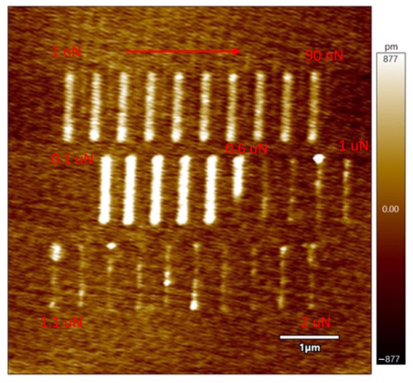
Figure 2. The lines scratched with different tip forces: Toplines are the forces ranging from 1 nN to 90 nN with an increment of 10 nN. Middle lines are the forces ranging from 0.1 μN to 1 μN with an increment of 0.1 μN. The bottom lines are the forces ranging from 1.1 μN to 2 μN with an increment of 0.1 μN. Image Credit: Mathew, et al., 2022
Figure 2 shows that the lines are very well defined and controlled for force values ranging from 0.1 μN. Figure 3 compares the consequences of oxide production at low and high relative humidity.
When the speed is low, the oxidation thickness is greater and broader, as shown in Figure 3A. The deposit’s height has risen to just above 4 nm at 200 nm/s, and it has increased to just above 1 nm at faster speeds. This is owing to the different speeds of the contact points between the tip and the substrate atoms.
Even though differing tip velocities cause inconsistent increments and decrements in height and depth, VT at 1 μm/s causes LAO with a constant increase in height and width until 9 V, after which a decline in both variables may be seen at 10 V, as illustrated in Figure 3B, C.
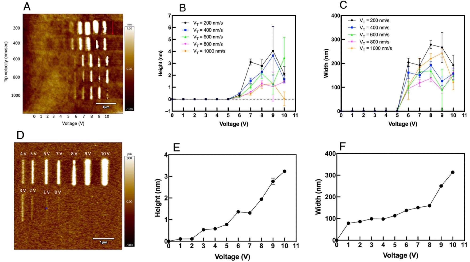
Figure 3. The lines are drawn on the surface under different humidity conditions: (A) The formation of oxide deposits with different tip velocities and voltage (B) The height vs. tip bias and (C) Width vs. tip bias of the lines scratched on the silicon surface. FT = 0.1 μN. RH is 36% (D) The lithographical lines drawn on the substrate with different voltages with a relative humidity of 75% and VT = 1 μm/sec. FT = 0.1 μN (E) The height vs. tip bias and (F) width vs. tip bias characteristics. Image Credit: Mathew, et al., 2022
The different lines painted on the silicon surface with a humidity range of 75–90% are shown in Figure 3D. It can be seen in Figures 3E and F that the width and height of the deposits on the surface are consistently increasing.
Figure 4 shows some of the letters drawn on the surface in a humid atmosphere with a RA of 75 percent. The letters are developed and distinct, and their thickness is consistent throughout. To summarise, LAO occurs with platinum-coated conductive tips and is influenced by tip velocity, tip bias, tip force, and humidity levels.
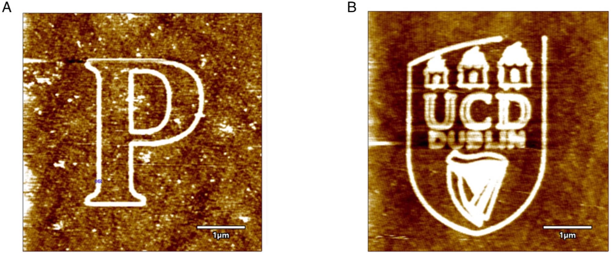
Figure 4. The intrinsic patterns fabricated over silicon substrate: (A) Letter ‘P’, and (B) UCD logo. FT = 0.1 μN and tip bias of 7 V, RH = 75%, VT = 1 μm/s. Image Credit: Mathew, et al., 2022
Figure 5 displays the contact mode scanned image of silicon in a 2 × 2 μm area, with a force of 2 μN. This force is active since it is used for employing nanolithography over hard substrates like silicon using single crystal diamond tips.
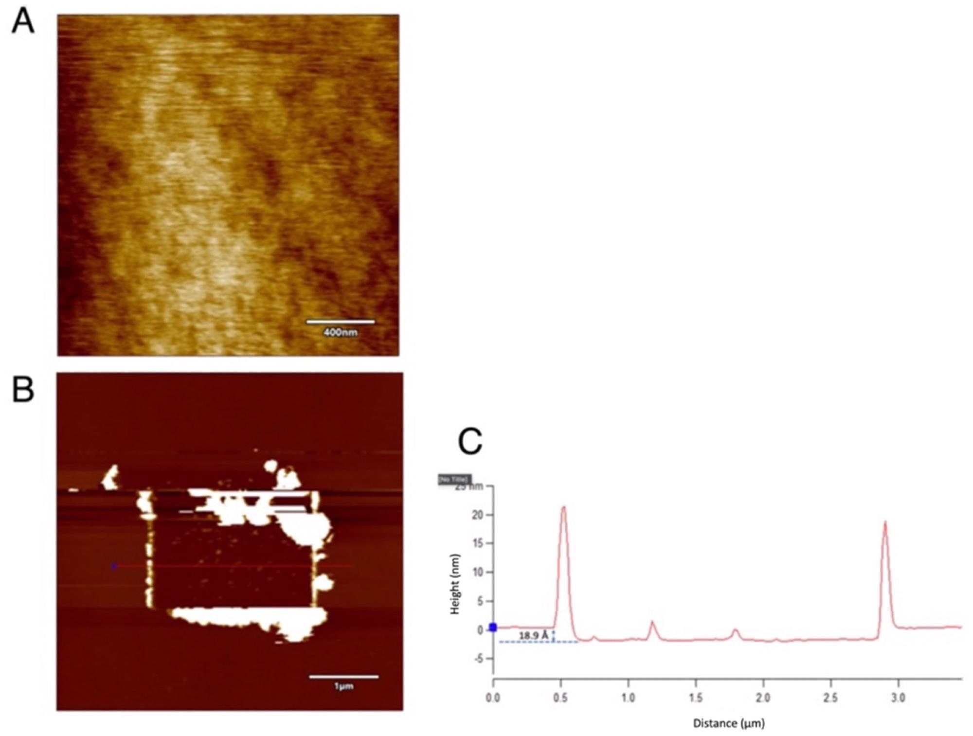
Figure 5. The contact mode scanning over silicon surface using a single crystal diamond tip: (A) The polished 2 × 2 μm area by contact mode scanning with a force of 2 μN. (B) The accumulation of debris on the sides and the (C) line profile show a depression of 1.89 nm. Tip bias: 0 V and RH ~75%. Image Credit: Mathew, et al., 2022
Figure 6 displays the lines scratched on this cleaned area with a marginally larger FT of 4 μN and diverse velocities ranging from 0 V to 10 V, with a VT of 1 μm/s. In the figure, stable and reliable material removal is attained for lower voltages to 6 V.
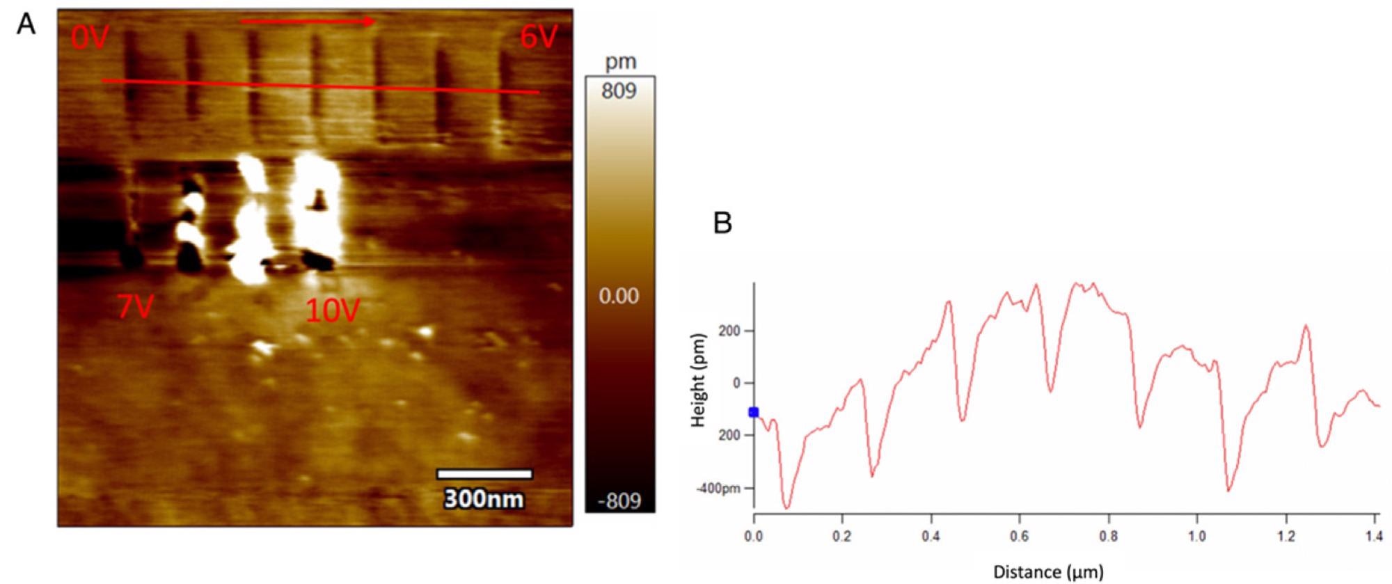
Figure 6. The scratched lines and the line profile with different tip voltages over a silicon substrate with a diamond tip: (A) The scratched lines over silicon using a single crystal diamond AFM tip with different tip voltages ranging from 0 V to 10 V with constant velocity (B) The line profile of the trenches (non-flattened). FT = 4 μN and the humidity is ~75%. Image Credit: Mathew, et al., 2022
A concentric square is scraped over the substrate under normal room circumstances (room humidity 25–30 %), as illustrated in Figure 7B, to learn more about the impact of material depth in various directions.
Some of the lines in Figure 7B are more noticeable, while others are less than that. Due to the obvious tip geometry, this is the reality. Figure 7A shows the SEM study of the diamond tip before scratching. Different sides of the analysis are shown as numbers in the figure for ease of understanding.
Figure 7B shows the same numbers as Figure 7A, representing the different sides of the AFM tip that pass through the scratching procedure, as indicated by the arrows. The lines are horizontally scanned with side 1 of the tip and retraced with side 3 of the tip when scanning is done at a 0° angle.
As shown by the line profile originating from the square’s center, depicted in Figure 7C, the square’s starting and ending points are substantially deeper.
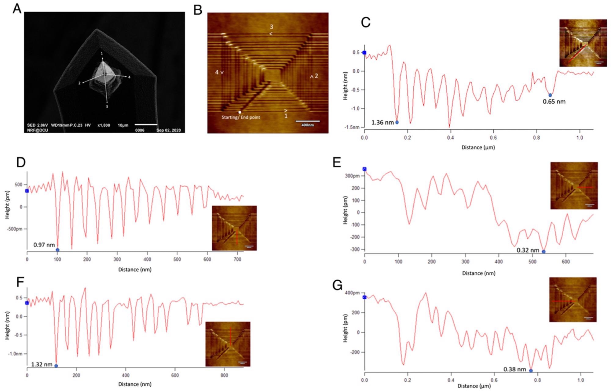
Figure 7. Analysis of different depth rates around the etched concentric square: (A) The SEM image of the diamond tip before scratching the silicon surface (B) The concentric square etched on the surface indicating the direction of tip motion and the sides of the tip with which the lines were in contact (C) The line profile along with the starting/endpoint, (D) The line profile along the rightward horizontal section where the AFM tip side 1 was in contact (E) The line profile along the upward vertical side where AFM tip side 2 was in contact (F) The line profile along the leftward horizontal plane where the AFM tip side 3 was in contact (G) The line profile along the downward vertical side of the concentric square where the AFM tip side 4 was in contact. The inset figures on the line profile show the representation of the lines on each side of the square. Image Credit: Mathew, et al., 2022
In the vertical direction, the materials are removed to a depth of less than 1 nanometer, falling as low as 0.32 nm in Figure 7E.
Experiments are carried out on a silicon substrate that has been dipped in a 10% HF solution to remove the natural oxide layer. The results are comparable to those obtained over bare silicon when the studies are carried out by drawing lines on the surface using a platinum-coated conductive tip, as illustrated in Figure 8.
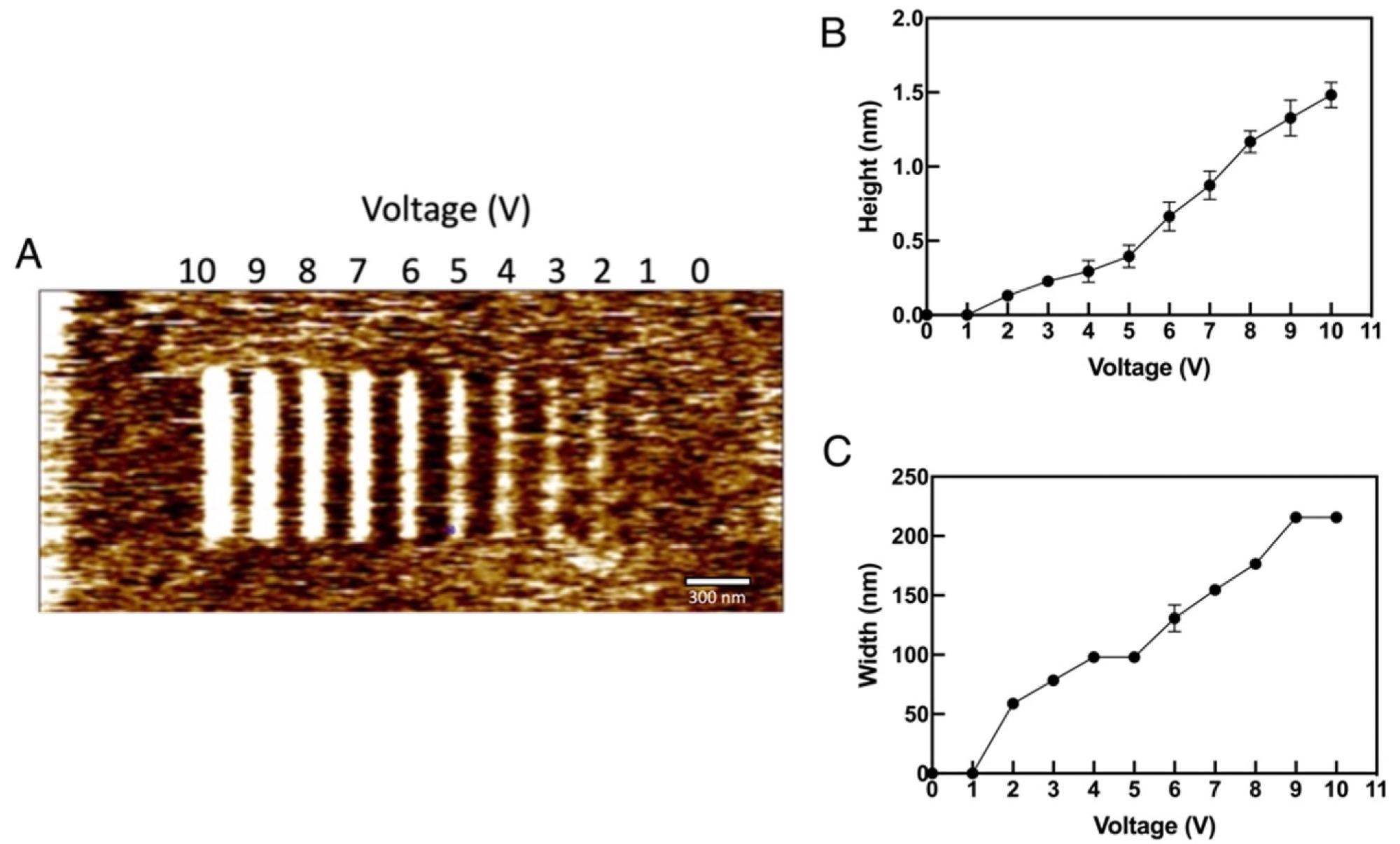
Figure 8. The LAO formation over HF treated silicon: (A) The formation of oxide deposits over HF treated silicon with different tip voltages ranging from 0 V to 10 V (B) The height vs. tip voltage characteristics and (C) The width vs. tip bias graph. FT = 0.1 μN, VT = 1 μm/s and RH ~26%. Image Credit: Mathew, et al., 2022
As illustrated in Figures 8B and C, the height and width of the oxide deposits are significantly more constant and regulated over the HF treated surface.
Material removal is done when the area is submitted to lithography using the diamond tip, on the other side. Figure 9A depicts the scratching of HF-treated silicon with three force values and voltages at 1 μm/s tip velocity, whereas Figure 9B depicts 3D imaging of the same surface. The material removal is accomplished directly over the substrate, as shown in the images.
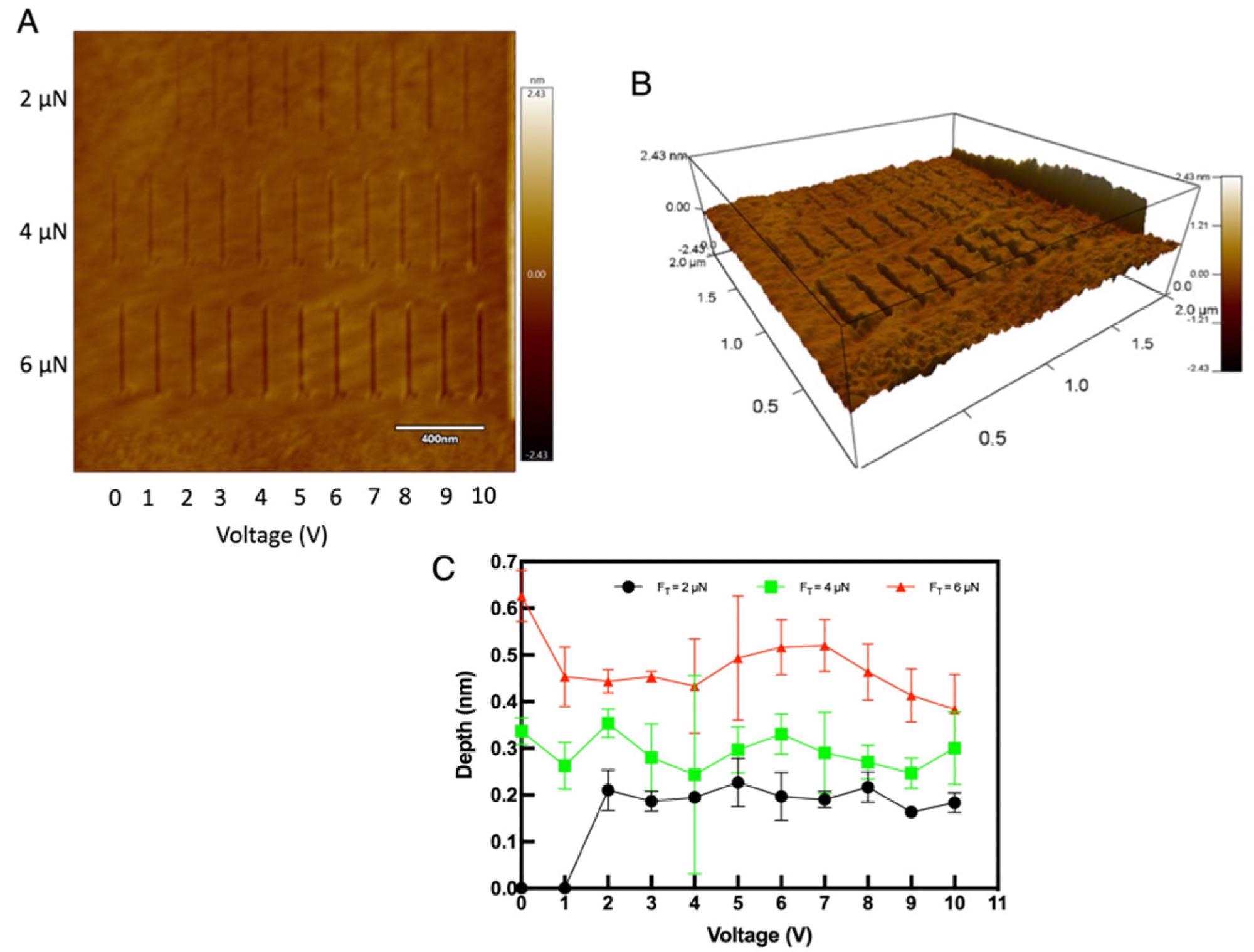
Figure 9. Scratching tests on HF treated silicon: (A) The etched lines on the silicon surface with different forces and voltages (B) The 3D image of the same where the etched depth can be seen increasing with higher force (C) The depth vas voltage graph showing the influence of different tip force. Image Credit: Mathew, et al., 2022
The impact of varied force values can be seen in Figure 9C. Depths as near to a single atomic layer can be attained with reduced force.
Conclusion
The effects of various factors on structure building over silicon (100) substrate employing two distinct AFM tips are investigated in depth. On the atomic scale, it has been discovered that with the right parameters, improved fabrication and material removal can be accomplished. Instead of removing material, a platinum-coated AFM tip depositions it on the substrate.
Furthermore, material removal with a diamond tip near the atomic scale is proven, as a depth of 0.32 nm, or around three silicon atoms, is achieved. Contact mode scanning can sweep the produced trash to the edges.
Since a smooth and uniform LAO is established, the relative humidity has a significant impact on the structure manufacturing. Material removal over bare silicon with a native oxide layer is found to be negatively associated with some depositions/surface damage, while it is uniform and clean over HF treated silicon. The diamond tip allows for direct material removal over bare silicon, whereas the platinum-coated tips necessitate a two-step technique.
This research lays the groundwork for future nanodevice fabrication, with applications ranging from the development of downsized electronic components to the mass manufacture of atomic-scale IC components, paving the way for the next generation of manufacturing.
Journal Reference:
Mathew, P. T., Han, W., Rodriguez, B. J., Fang, F. (2022) Structure Fabrication on Silicon at Atomic and Close-To-Atomic Scale Using Atomic Force Microscopy: Implications for Nanopatterning and Nanodevice Fabrication. Micromachines, 13(4), p. 524. Available Online: https://www.mdpi.com/2072-666X/13/4/524/htm.
References and Further Reading
- Avouris, P., et al. (1997) Atomic Force Microscope Tip-Induced Local Oxidation of Silicon: Kinetics, Mechanism, and Nanofabrication. Applied Physics Letters, 71(2), pp. 285–287. doi.org/10.1063/1.119521.
- Bo, X. -Z., et al. (2002) Nanopatterning of Si/SiGe Electrical Devices by Atomic Force Microscopy Oxidation. Applied Physics Letters, 81(17), pp. 3263–3265. doi.org/10.1063/1.1515113.
- Avouris, P., et al. (1998) AFM-Tip-Induced and Current-Induced Local Oxidation of Silicon and Metals. Applied Physics A, 66, pp. S659–S667. doi.org/10.1007/s003390051218.
- Losilla, N. S., et al. (2009) Large Area Nanoscale Patterning of Silicon Surfaces by Parallel Local Oxidation. Nanotechnology, 20(47), p. 475304. doi.org/10.1088/0957-4484/20/47/475304.
- Miyake, S & Kim, J (2001) Fabrication of Silicon Utilizing Mechanochemical Local Oxidation by Diamond Tip Sliding. Japanese Journal of Applied Physics, 40(11B), pp. L1247–L1249. doi.org/10.1143/JJAP.40.L1247.
- Tello, M & García, R (2001) Nano-Oxidation of Silicon Surfaces: Comparison of Noncontact and Contact Atomic-Force Microscopy Methods. Applied Physics Letters, 79(3), pp. 424–426. doi.org/10.1063/1.1385582.
- Notargiacomo, A & Tseng, A A (2009) Assembling Uniform Oxide Lines and Layers by Overlapping Dots and Lines Using AFM Local Oxidation. In: 2009 9th IEEE Conference on Nanotechnology (IEEE-NANO), Genoa, Italy, 26–30 July 2009; pp. 907–910. Available at: https://ieeexplore.ieee.org/abstract/document/5394609.
- Mathew, P. T., et al. (2020) Atomic and Close-to-Atomic Scale Manufacturing: A Review on Atomic Layer Removal Methods Using Atomic Force Microscopy. Nanomanufacturing and Metrology, 3, pp. 167–186. doi.org/10.1007/s41871-020-00067-2.
- Yamamoto, K., et al. (2017) Localized Etching of Silicon in Water Using a Catalytically Active Platinum-Coated Atomic Force Microscopy Probe. Precision Engineering, 50, pp. 344–353. doi.org/10.1016/j.precisioneng.2017.06.008.
- Zheng, H., et al. (2013) Electron Beam-Assisted Healing of Nanopores in Magnesium Alloys. Scientific Reports, 3, p. 1920. doi.org/10.1038/srep01920.
- Aramesh, M (2018) Ion-Beam Sculpting of Nanowires. Physica Status Solidi Rapid Research Letters, 12(1), p. 1700333. doi.org/10.1002/pssr.201700333.
- Chen, W., et al. (2018) Cutting Mechanism Investigation in Vibration-Assisted Machining. Nanomanufacturing and Metrology, 1, pp. 268–276. doi.org/10.1007/s41871-018-0031-x.
- Heidari, M., et al. (2019) Effects of Tool Rake Angle and Tool Nose Radius on Surface Quality of Ultraprecision Diamond-Turned Porous Silicon. Journal of Manufacturing Processes, 37, pp. 321–331. doi.org/10.1016/j.jmapro.2018.12.003.
- Dahlman, P., et al. (2004) The Influence of Rake Angle, Cutting Feed and Cutting Depth on Residual Stresses in Hard Turning. Journal of Materials Processing Technology, 147(2), pp. 181–184. doi.org/10.1016/j.jmatprotec.2003.12.014.
- Rahman, M. A., et al. (2017) Variation of Surface Generation Mechanisms in Ultra-Precision Machining Due to Relative Tool Sharpness (RTS) and Material Properties. International Journal of Machine Tools and Manufacture, 115, pp. 15–28. doi.org/10.1016/j.ijmachtools.2016.11.003.
- Wang, M & Duan, F (2021) Atomic-Level Material Removal Mechanisms of Si(110) Chemical Mechanical Polishing: Insights from ReaxFF Reactive Molecular Dynamics Simulations. Langmuir, 37(6), pp. 2161–2169. doi.org/10.1021/acs.langmuir.0c03416.
- Liu, C., et al. (2021) Molecular Dynamics Simulation on Cutting Mechanism in the Hybrid Machining Process of Single-Crystal Silicon. Nanoscale Research Letters, 16, p. 66. doi.org/10.1186/s11671-021-03526-x.
- Yue, X & Yang, X (2015) Molecular Dynamics Simulation of the Material Removal Process and Gap Phenomenon of Nano EDM in Deionized Water. RSC Advances, 5(82), pp. 66502–66510. doi.org/10.1039/C5RA11419E.
- Fang, F Z (2020) Atomic and Close-to-Atomic Scale Manufacturing: Perspectives and Measures. International Journal of Extreme Manufacturing, 2(3), p. 030201. doi.org/10.1088/2631-7990/aba495.
- Xie, W & Fang, F Z (2020) On the Mechanism of Dislocation-Dominated Chip Formation in Cutting-Based Single Atomic Layer Removal of Monocrystalline Copper. The International Journal of Advanced Manufacturing Technology, 108, pp. 1587–1599. doi.org/10.1007/s00170-020-05527-z.
- Xie, W & Fang, F Z (2020) Mechanism of Atomic and Close-to-Atomic Scale Cutting of Monocrystalline Copper. Applied Surface Science, 503, p. 144239. doi.org/10.1016/j.apsusc.2019.144239.
- Xie, W & Fang, F Z (2020) Effect of Tool Edge Radius on Material Removal Mechanism in Atomic and Close-to-Atomic Scale Cutting. Applied Surface Science, 504, p. 144451. doi.org/10.1016/j.apsusc.2019.144451.
- Xie, W & Fang, F Z (2019) Cutting-Based Single Atomic Layer Removal Mechanism of Monocrystalline Copper: Atomic Sizing Effect. Nanomanufacturing and Metrology, 2, pp. 241–252. doi.org/10.1007/s41871-019-00045-3.
- Xie, W & Fang, F Z (2019) Cutting-Based Single Atomic Layer Removal Mechanism of Monocrystalline Copper: Edge Radius Effect. Nanoscale Research Letters, 14, p. 370. doi.org/10.1186/s11671-019-3195-4.
- Chen, L., et al. (2018) Nanomanufacturing of Silicon Surface with a Single Atomic Layer Precision via Mechanochemical Reactions. Nature Communications, 9, p. 1542. doi.org/10.1038/s41467-018-03930-5.
- Han, W., et al. (2022) Toward Single-Atomic-Layer Lithography on Highly Oriented Pyrolytic Graphite Surfaces Using AFM-Based Electrochemical Etching. Nanomanufacturing and Metrology, 5, pp. 32–38. doi.org/10.1007/s41871-022-00127-9
- Matei, G. A., et al. (2006) Precision and Accuracy of Thermal Calibration of Atomic Force Microscopy Cantilevers. Review of Scientific Instruments, 77(8), p. 083703. doi.org/10.1063/1.2336115
- Zhang, F., et al. (2020) Investigation of AFM-Based Machining of Ferroelectric Thin Films at the Nanoscale. Journal of Applied Physics, 127(3), p. 034103. doi.org/10.1063/1.5133018.
- Kim, U. S., et al. (2017) The Possibility of Multi-Layer Nanofabrication via Atomic Force Microscope-Based Pulse Electrochemical Nanopatterning. Nanotechnology, 28(19), p. 195302. doi.org/10.1088/1361-6528/aa6954.
- Dehzangi, A., et al. (2013) Impact of Parameter Variation in Fabrication of Nanostructure by Atomic Force Microscopy Nanolithography. PLoS ONE, 8(6), p. e65409. doi.org/10.1371/journal.pone.0065409.
- Cabrera, N & Mott, N F (1949) Theory of the Oxidation of Metals. Reports on Progress in Physics, 12(1), pp. 163–184. doi.org/10.1088/0034-4885/12/1/308.
- Temiryazev, A (2014) Pulse Force Nanolithography on Hard Surfaces Using Atomic Force Microscopy with a Sharp Single-Crystal Diamond Tip. Diamond and Related Materials, 48, pp. 60–64. doi.org/10.1016/j.diamond.2014.07.001