Semiconductor materials play an important part in developing nanophotonic technologies. Semiconductors are used for generating controllable photons as well as for confining and exploiting them for useful applications.

Image Credit: agsandrew/Shutterstock.com
The backbone of the digital revolution that has dictated the world over the last half a century is based on the properties of semiconductors. Semiconductors showcase unique electrical characteristics that can be manipulated to perform many tasks required for computing and data processing. The flow of electrons - electricity - behaves differently in a semiconductor than in a metal. Being able to control the electrons results in devices that are commonly referred to as electronics.
Semiconductors also exhibit unique optical properties that can be leveraged for various impactful applications. Light is produced by photons. Technology developed by manipulating and controlling photons is known as photonics. A specialized branch of photonics called nanophotonics or nano-optics studies how light behaves at nanometer scales as well as how nanometer-sized objects interact with light.
Properties of Semiconductors
Semiconductors are defined as materials with electrical conduction properties that fall between insulators and conductors. The elements silicon (Si), germanium (Ge) and indium (In) are a few examples of semiconductors.
Semiconductors are divided into intrinsic semiconductors and extrinsic semiconductors. Chemically pure semiconductors with no impurities, like the examples above, are called intrinsic semiconductors. With intrinsic semiconductors, rather than impurities, the characteristics of the material itself control how many electrons and holes are present. Electrons are negatively charged elementary charge carriers and holes are positively charged vacancies in semiconductors. The amount of excited electrons equals the number of holes in intrinsic semiconductors.
Electrical and optical characteristics of an extrinsic semiconductor are modified by adding certain impurities. Dopants change the number of protons or electrons to meet specific requirements. These alloy semiconductors are also known as compound semiconductors and are suitable for electrical and optoelectronic applications. Some examples of extrinsic semiconductors are gallium nitride (GaN), indium phosphide (InP), and gallium arsenide (GaAs). Such extrinsic semiconductors have become prominent materials from which photon-confining devices like waveguides are constructed. Waveguides have been shown to transfer entangled photons efficiently for applications in quantum information sciences.
Internal Structure and Optical Nature of Semiconductors
Lattice and the electronic features of semiconductors give them their optical properties. The vibrations in lattice-ionic crystals are responsible for the optical lattice properties of semiconductors. Due to the interaction between light and optical phonons - vibrations in the lattice - they exhibit significant infrared absorption and reflection.
The electronic states of semiconductors are the focus of optical-electronic properties. A semiconductor's energy bands are its electronic states. The valence and conduction bands are the primary energy states in a semiconductor that is taken advantage of for creating innovative nanophotonics technology.
The semiconductor's electron-occupied outermost energy level is known as the valence band. By applying the appropriate amount of energy, electrons in the valence band's orbitals are excited into the conduction band.
When exposed to sufficient energy, valence band electrons can be excited to the electron orbitals that make up the conduction band. Electrons in the conduction band can flow freely inside the semiconductor. Here, a hole forms in an electron's vacancy when it leaves the valence band for the conduction band. Moreover, positively charged holes can also travel freely inside the material.
When stimulated by photons, semiconductor electrons switch between two energy levels. Optical transitions in atoms are comparable to this phenomenon. Interband transitions are between the conduction and valence bands. In the region between these two bands, there is the potential for absorption, stimulated emission, and spontaneous emission.
When a photon is absorbed by a semiconductor, it results in optical absorption. The photon energy must be either equal to or greater than the energy of the band gap for absorption to occur. The difference in energy between the valence and conduction levels is known as the band gap energy. An electron and a hole are produced in the valence and conduction bands by absorption.
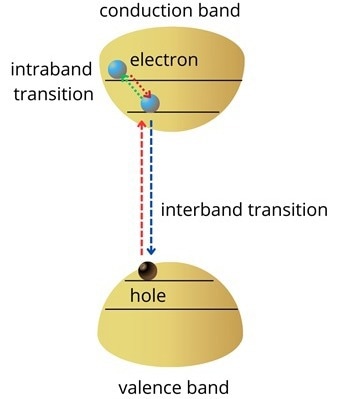
Figure 1. Schematic of a semiconductor’s energy band structure. Credit: Ilamaran Sivarajah
The lowest energy level on the conduction band will be quickly filled by electrons produced with higher energy than the band gap. Also, holes created in the valence band will rise to the top of the valence band, as illustrated in Figure 1. Intraband transitions are the energy levels at which electrons change within the conduction or valence bands. Nanophotonics has benefited greatly from technology that has been developed by exploiting intraband transitions.
Semiconductors also exhibit spontaneous and stimulated emissions. When an electron from the conduction level transitions back into the valence band, spontaneous emission, also known as optical recombination, occurs, producing a photon in the process. There are no interactions with any additional photons during spontaneous emission, which occurs naturally and at random. Additional optical pumping is employed to transfer electrons between the two energy levels.
New possibilities in nanophotonics have emerged with the development of atomically thin layers of bonded semiconductor materials. Semiconductor transition metal dichalcogenides (TMDs) are one of them. These materials have been shown to have direct bandgaps in the monolayer limit, which makes them ideal for applications in photonics and optoelectronics.
Monolayers of TMDs consist of one layer of a specific atom sandwiched between two layers of a different type of atom. These two-dimensional materials can not only substitute for conventional materials like Si or GaAs in conventional electronic or photonic devices, but they can also possess unique physical properties like spin-valley physics, which are currently being investigated for "valleytronics" and coherent quantum bits. Additionally, heterostructures not constrained by lattice mismatch between adjacent layers, as is the case with conventional semiconductors, can be created by stacking the individual layers of various 2D crystals. This makes it possible to engineer nanophotonics with specific properties in numerous ways.
Outlook
The versatility offered by semiconductor materials has created new opportunities for a number of nanophotonic applications in light harvesting, sensing, quantum technology, optical switching, and biological diagnostics. Nanophotonic structures are the catalyst for the upcoming economic frontier and are positioned to be the cornerstone of the quantum revolution as it previously underpinned the digital age.
References and Further Reading
Sivarajah, I. Recent Developments in Optical Semiconductors. [Online] AZoOptics.com. Available at: https://www.azooptics.com/Article.aspx?ArticleID=2217
Mak, K., Shan, J. (2016) Photonics and optoelectronics of 2D semiconductor transition metal dichalcogenides. Nature Photon 10, pp. 216–226 . https://doi.org/10.1038/nphoton.2015.282
Muhammad Aamir Iqbal, Naila Ashraf, Wajeehah Shahid, Muhammad Awais, Abdullah Khan Durrani, Khurram Shahzad and Mujtaba Ikram. (2021) Nanophotonics: Fundamentals, Challenges, Future Prospects and Applied Applications. Nonlinear Optics. doi.org/10.5772/intechopen.98601
Lu, W., Fu, Y. (2018). Introduction to Physics and Optical Properties of Semiconductors. In: Spectroscopy of Semiconductors. Springer Series in Optical Sciences, Springer, Cham. 215. https://doi.org/10.1007/978-3-319-94953-6_2
usechatgpt init success
Disclaimer: The views expressed here are those of the author expressed in their private capacity and do not necessarily represent the views of AZoM.com Limited T/A AZoNetwork the owner and operator of this website. This disclaimer forms part of the Terms and conditions of use of this website.