Reviewed by Maria OsipovaOct 5 2023
In this interview, AZoNano speaks with Chris Schwalb about SEM, AFM, and the development and significance of FusionScope in the realm of nanoscale analysis.
Please could you introduce yourself and your role at Quantum Design Microscopy?
My name is Chris Schwalb, and I lead the Quantum Design Microscopy team at our European Headquarters in Darmstadt, Germany. I have been working in the field of correlative microscopy for more than 15 years and love exciting technology. Therefore, I am thrilled to introduce our latest development – the FusionScope™ – the first truly correlative AFM-SEM microscopy platform.
Why are SEM and AFM so complementary to one another?
SEM and AFM are extremely complementary and two of the most powerful microscopy techniques currently available. AFM offers real 3D topography information with sub-nm resolution, something that SEMs can only provide indirectly. In addition, AFM can also provide information on nano-mechanical properties, as well as magnetic and electrical characterization of samples, which is a blind spot for the SEM. On the other hand, AFMs are “chemically blind.”
Here, the SEM, in combination with EDX/EDS, can provide a detailed chemical analysis of the sample surface. In addition, SEM offers a wide field of view, which is critical in identifying regions of interest with feature sizes of less than a micron. These are notoriously difficult to find over larger spatial scales in conventional AFM systems.
With the help of the high-resolution SEM, the AFM cantilever tip can be precisely navigated by the User to the desired sample area, even for challenging three-dimensional topologies. By combining all of these methods into one instrument, you get the best of both worlds.
Could you discuss the background behind the FusionScope’s creation?
The FusionScope story began almost ten years ago when Mike Simmonds – one of the co-founders of Quantum Design – started the groundbreaking work on the e-scope, which was a miniature scanning electron microscope column that he developed pretty much by himself in his lab. He inquired about the potential for this new column to serve as a complementary key capability within a highly integrated instrument, aiming to enhance the facilitation of correlative microscopy.
In addition, in 2018, Quantum Design completed the acquisition of GETec – a small Austrian company that I worked for at the time. We developed a small and compact AFM scanner that could be integrated into the high-vacuum environment of stand-alone SEM systems.
This led to the vision for a combined AFM/SEM instrument that seamlessly connects both worlds in an intuitive, easy-to-use, and efficient way and was the start of the FusionScope development.
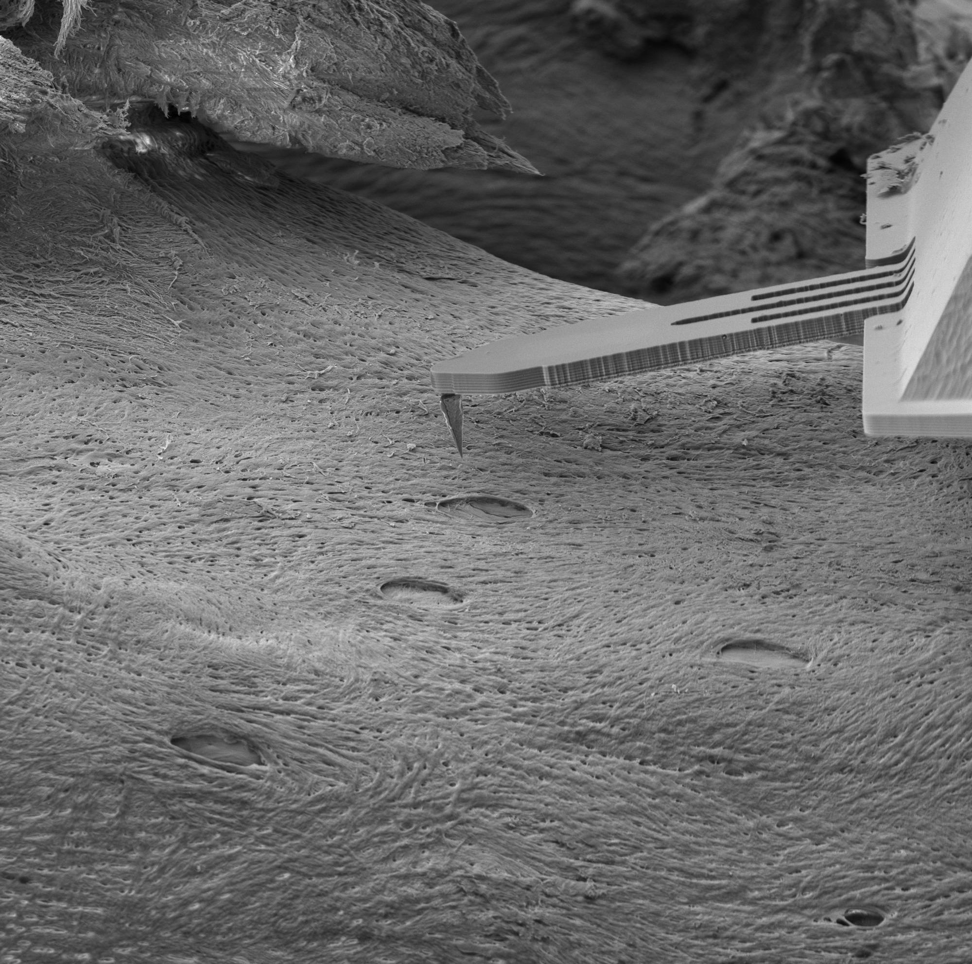
Image Credit: Quantum Design
The FusionScope offers users a fully integrated correlative microscopy platform combining SEM imaging with AFM measurement methodologies. Why is this product so exciting for nanoscale analysis?
The FusionScope is very exciting for nanoscale analysis because it is the first true correlative microscopy platform designed from the ground up to seamlessly add the benefits of SEM imaging to a wide range of AFM measurement techniques.
This allows users to perform direct in-situ combinations of these complimentary techniques due to the simultaneous operation of SEM and AFM inside one single vacuum chamber. Especially exciting is the capability to precisely navigate the AFM cantilever tip via the SEM, which enables users to analyze hard-to-reach sample areas or easily locate nanometre-sized objects and structures on your sample surface.
In addition, all of the AFM and SEM data can be directly correlated and combined within a single software interface using FusionScope’s joint coordinate system.
Could you run through the suite of characterization techniques the FusionScope offers?
FusionScope offers all standard SEM and AFM characterization techniques. The AFM provides contact mode, dynamic mode, magnetic and conductive measurements, and the analysis of mechanical properties. This enables the user to characterize the real 3D sample topography and study the mechanical, magnetic, and electrical properties of the sample. All these AFM modes can be combined with the standard SEM capabilities.
What are some of the highlight applications of the FusionScope, and what makes it stand out from other commercially available equipment?
FusionScope offers the user a broad range of applications in many different fields of research and development, including material characterization, the study of nanostructures, quality control, and failure analysis.
Different nanostructures such as nanowires, 2D materials, and nanoparticles can be easily characterized. We have customers that study individual nanowires on TEM grids where it is crucial to have the SEM for locating the nanowire and afterward positioning the AFM tip on the TEM grid.
In the fields of quality control and failure analysis, we have customers who want to combine nanoprobing capabilities with conductive or magnetic AFM measurements to study semiconductor devices.
In this way, FusionScope breaks with the traditional conventions and boundaries typically used for sequential AFM and SEM analysis and improves the capabilities, performance, and ease of use by allowing interactive in-situ correlative microscopy. It saves the user a significant amount of time by enabling both SEM and AFM analysis in a single platform.
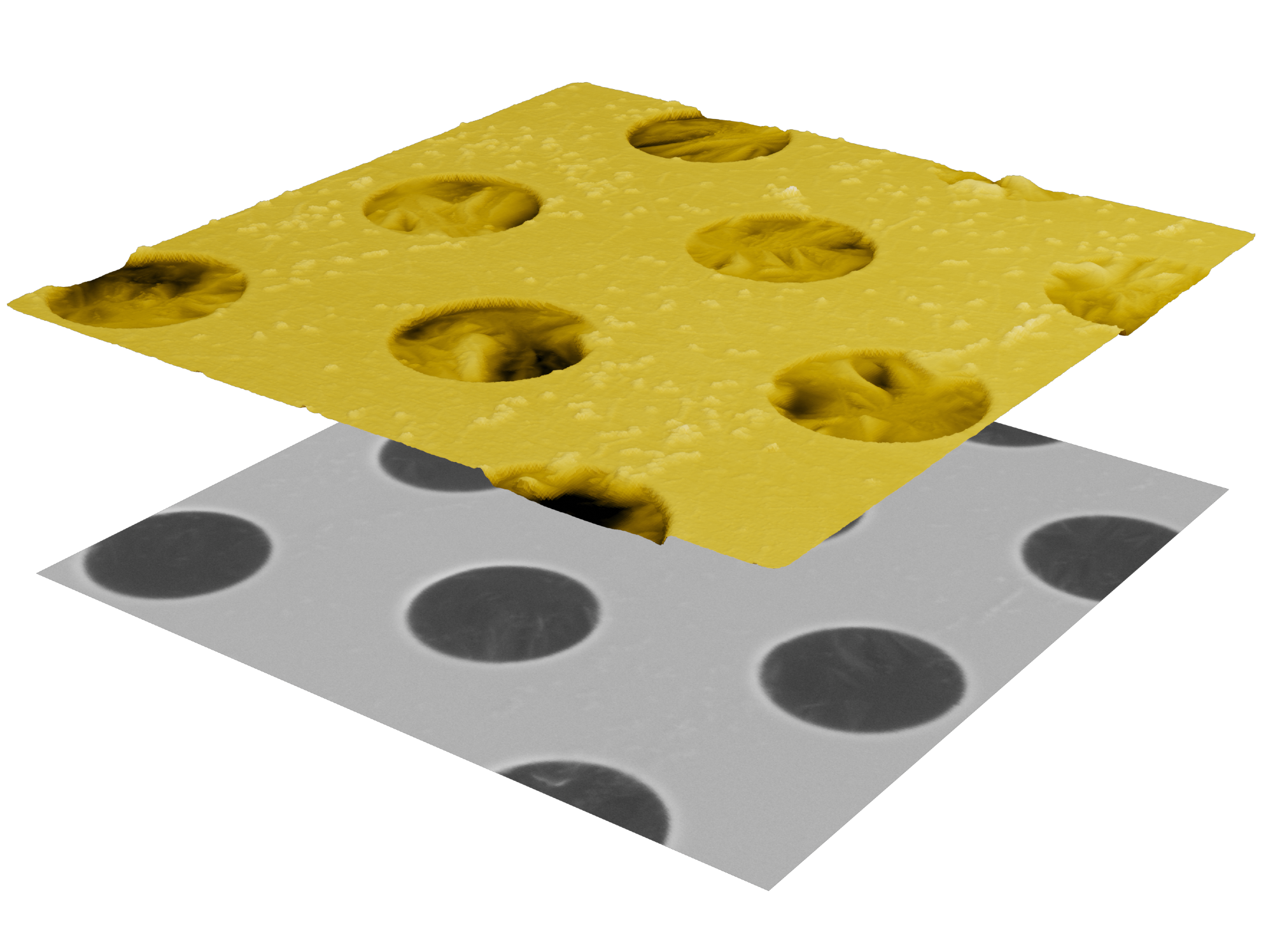
Image Credit: Quantum Design
One of the key technical components of the FusionScope is its correlated coordinate system. Could you discuss how this system improves the user experience?
The correlated coordinate system is at the core of FusionScope, playing a pivotal role in providing an intuitive user experience. It seamlessly integrates AFM and SEM operations, ensuring that all measurements and tracking utilize the same precise 'map' for sample measurements and locating specific areas of interest.
This capability also enables automated features in FusionScope software, such as locating an area of interest using SEM and then instructing the FusionScope to automatically find the same area with the AFM. For users, this not only saves time but also enables a completely new and interactive approach to conducting AFM and SEM analyses.
What other features of the FusionScope make it an accessible, high-performance analysis tool?
One of the distinctive features of FusionScope is the Profile View, which allows users to observe the AFM cantilever's tip during measurements and precisely position it on the area of interest on the sample.
This is made possible because the AFM scan head and the sample holder share a trunnion, allowing both parts to be tilted simultaneously within a range of -10° to +80° relative to the SEM beam. Being able to observe the actual AFM tip in real time is a game-changer for conducting AFM analysis, as it enables users to closely monitor the tip's movements while using the SEM.
Integral to the FusionScope concept is the utilization of piezoresistive cantilevers with electric self-sensing cantilever deflection readout. This technology enables high-quality, low-noise detection of surface properties without the need for optical alignment. These advantages directly contribute to improved performance and user-friendliness, allowing users to swiftly change AFM tips and allocate more time to image recording.
In addition, FusionScope is designed for fast sample exchange and mechanical and thermal robustness. Samples can be swapped by the user in less than a few minutes and single atomic steps can be easily resolved.
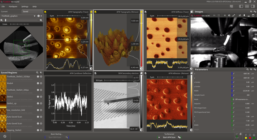
Image Credit: Quantum Design
Are users able to customize the FusionScope to expand its technical capabilities?
FusionScope’s design principle offers a modular architecture that allows for the easy expansion of measurement techniques and modes by providing extra chamber ports that enhance the system’s capabilities. For example, Energy Dispersive X-Ray Spectroscopy (EDS/EDX), a Backscatter Detector (BSE), or nano-probing via nano-manipulators can be easily upgraded.
In addition, FusionScope allows the user to use Python scripting to create customized workflows for specific measurement tasks.
Could you discuss some case studies involving the FusionScope?
Despite its relatively brief presence on the market, FusionScope has already been employed in several case studies that have resulted in scientific publications. These case studies have encompassed detailed characterization of individual nanowires for energy harvesting, examining pharmaceutical nanoparticles, and measuring magnetic properties in 3D structures, among others.
What are the next steps for the FusionScope’s journey?
Quantum Design has ventured into a wholly new market with the introduction of the FusionScope, a unique product distinct from our typical customer base. We are thrilled to have initiated this groundbreaking shift in correlative microscopy, where our goal is to elevate AFM and SEM capabilities to new heights in various applications.
We want to grow these abilities by adding exciting new features and measurement options to make FusionScope a game-changer for correlative analysis in the future.
About Chris Schwalb 
Chris Schwalb is the product manager and head of the FusionScope application team at Quantum Design Microscopy. Throughout his professional career he worked on the development of new 3D nanoprinting processes, sensors, and in-situ microscopy techniques. He obtained his Ph.D. in Surface Physics at Philipps University in Marburg studying electron transfer processes at metal-organic interfaces.

This information has been sourced, reviewed and adapted from materials provided by Quantum Design Microscopy GmbH.
For more information on this source, please visit Quantum Design Microscopy GmbH.
Disclaimer: The views expressed here are those of the interviewee and do not necessarily represent the views of AZoM.com Limited (T/A) AZoNetwork, the owner and operator of this website. This disclaimer forms part of the Terms and Conditions of use of this website.