In 1975, American engineer Gordon Moore famously predicted that the densities of semiconductor chips would double every two years. This prediction eventually came to pass over the next two decades and it became known as Moore's Law.
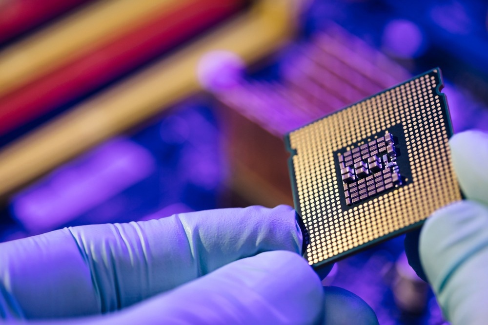
Image Credit: mpohodzhay/Shutterstock.com
The advancement of semiconductor technology kept pace with Moore's Law until around the year 2000, when physical limitations created a significant bottleneck. However, a 2007 breakthrough in three-dimensional semiconductor architecture broke open this bottleneck, and Moore's law has largely held true to this day.
Before passing away in March 2023, Moore said that his prediction was a lucky guess that was never meant to become known as a “law,” per se. However, he continued to advocate for silicone as the semiconductor vehicle through which Moore's Law would continue to hold.
Moore also expressed skepticism about quantum computing technology beyond niche applications, and the American engineer never gave public support to the idea of nanomaterials being the successor to silicon; downsizing would eventually push semiconductors to the atomic scale.
The Rise of Nanoscale Chips
Today, it appears we are on the precipice of another bottleneck. Researchers are increasingly looking to nanotechnology as a way to extend Moore's law and continue advancing semiconductor technology. Some of the most popular efforts are focused on two-dimensional semiconductors, and the growing number of advocates for this technology now includes industry giants like Intel and the Taiwan Semiconductor Manufacturing Company (TSMC).
In 2022, TSMC announced plans to build a $33-billion factory that would produce the world's first 2-nanometer semiconductor chips. These chips would be faster and about 30% more efficient than existing microchip technology. The factory is expected to start production in 2025 and many chips will likely be bought by Apple, TSMC’s biggest customer.
One promising area of research is focused on transition metal dichalcogenides (TMDs), particularly molybdenum disulfide (MoS2). As a semiconductor, this material has a bandgap that can be tuned by adding or removing the number of layers. Research efforts have been focused on large-scale demonstrations that use MoS2 in conjunction with the current semiconductor manufacturing process.
MoS2 research efforts are focused on processing at the scales of two nanometers and smaller, which is far below the diffraction limit of visible light of around 200 nm. To address this limitation, the Dutch company ASML is currently developing a system based on extreme ultraviolet light (EUV) that has a wavelength of 13.5 nm.
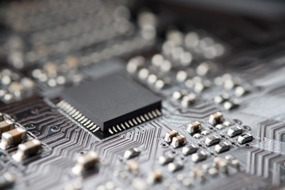
Image Credit: megaflopp/Shutterstock.com
Pushing the known boundaries of physics, devices from ASML use EUV light created by firing a laser into liquid tin and bouncing that laser light off precision-made mirrors that are said to be the flattest surfaces in the world. The entire system costs more than $150 million and it has to be shipped in 40 massive freight containers using three cargo planes and over 20 trucks. Despite the cost and logistics, ASML has sold more than 140 of these cutting-edge systems, according to Physics World.
Google and Amazon are some of the first companies to use semiconductors with EUV features. According to MIT Technology Review, these chips are being used for photo recognition, language translation, search engine results, and AI technology. Chips from ASML are also already being used phones from Apple and Samsung.
Other Nanotech Driving Moore Law Today
Other efforts are also underway to continue advancing semiconductor technology, and by extension Moore's Law.
Fin field-effect transistors (FinFETS) involve the use of fin-like structures on the silicone base. These structures allow for transistors to be stacked on top of each other, and some devices have more than 175 mask layers. The semiconductor industry is expected to be able to leverage FinFETS technology to make devices with more than 600 layers in the very near future.
Gate all around (GAA) devices are another cutting-edge semiconductor technology operating at the two-nanometer scale. Essentially a silicon nanowire with a gate wrapped around it, GAA technology is being used by IBM to create semiconductors with 333 million transistors on one square millimeter. IBM has said it can fit 50 billion transistors on a semiconductor chip the size of a fingernail. The company says these chips could make laptops run faster, quadruple smartphone battery life, and reduce data center costs.
Using these technologies and others, companies are doing everything they can to continue advancing semiconductor technology and maintain Moore's Law. And there is still significant room for improvement. With the distance between gates at around 50 nanometers, two-nanometer technology has significant room to work with. Engineers can also create software that is more efficient to get more processing power out of existing technology.
As it currently stands, extending Moore's Law may not be as much a matter of physics, as a matter of economics. The upcoming TSMC factory will cost around $33 billion, which is $10 to $15 billion more than the cost of plants making five-nanometer semiconductor technology. Only a handful of companies are capable of spending this kind of money to advance semiconductor technology.
References and Further Reading
Liu, S., Hu et al. (2023). High-performance MoS2 nanotransistors with record low subthreshold swing and high on-current. Nature Nanotechnology, 18(6), 678-684. https://www.nature.com/articles/s41565-023-01411-5
McKenzie, J. (2023, October 6). Moore's law: further progress will push hard on the boundaries of physics and economics. Physics World. https://physicsworld.com/a/moores-law-further-progress-will-push-hard-on-the-boundaries-of-physics-and-economics
IBM. (2021, May 6). IBM Unveils World's First 2 Nanometer Chip Technology, Opening a New Frontier for Semiconductors. IBM Newsroom. https://newsroom.ibm.com/2021-05-06-IBM-Unveils-Worlds-First-2-Nanometer-Chip-Technology,-Opening-a-New-Frontier-for-Semiconductors
Disclaimer: The views expressed here are those of the author expressed in their private capacity and do not necessarily represent the views of AZoM.com Limited T/A AZoNetwork the owner and operator of this website. This disclaimer forms part of the Terms and conditions of use of this website.