Semiconductor chips, which have thus far dominated the electronics industry, are now reaching practical and fundamental limits. Novel alternatives are therefore required to overcome these limits and allow the continuity of Moore’s law.
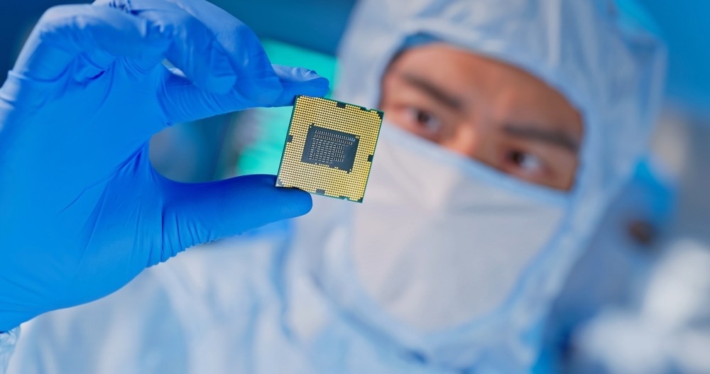
Image Credit: aslysun/Shutterstock.com
Materials beyond silicon (Si), such as Group III-V and other nanomaterials, are being aggressively integrated into electronics. Two-dimensional (2D) materials like graphene and transition metal dichalcogenides (TMDs) also exhibit great potential in nanoscale devices.1
This article explores novel classes of third-generation semiconductors, organic semiconductors, flexible electronics, and other potential alternatives to conventional semiconductor chips.1,2
Emerging Materials for Semiconductor Devices
Semiconductor chips are critical components in electronic devices, medical equipment, and sensors.2 Accordingly, the conventional Si complementary metal-oxide-semiconductor (CMOS) technology has been scaled to high-performance fin field-effect transistors (FinFETs). However, further performance enhancement is plateauing with the continued use of Si.1
With rising environmental concerns, there is a global shift toward energy-efficient electronics.2 The processing of traditional Si-based electronics is problematic due to the use of toxic and non-recyclable components and the release of hazardous by-products.3
Thus, future sustainable electronics scaling requires alternative materials, such as wide bandgap semiconductors, 2D materials, TMDs, organic semiconductors, quantum dots, and other nanomaterials.
Beyond Silicon: Gallium Nitride and Silicon Carbide
Third-generation semiconductors (with a bandgap greater than 2.3 electron volts), such as silicon carbide (SiC), gallium nitride (GaN), zinc oxide, aluminum nitride, and diamond, are crucial in fulfilling the rising demand for alternatives to Si.
They exhibit superior thermal conductivity, high bonding energy, rapid electron mobility, and robust breakdown field strength. Their high-temperature endurance and resistance to radiation are added advantages.2
Among various third-generation semiconductors, GaN and SiC are the most promising alternatives to Si chips. They boast a bandgap three times that of their first and second-generation counterparts and can handle high-voltage and high-power applications.
SiC metal-oxide-semiconductor field-effect transistors (MOSFETs) and GaN high-electron-mobility transistors (HEMTs) are replacing conventional chips in high-power and high-frequency applications, respectively.2
Organic Semiconductors and Flexible Electronics
Organic large-area electronics are rapidly advancing as a flexible and customizable alternative to conventional semiconductor chips. Although Si can be processed into solution form for printing, it requires a high annealing temperature, making it incompatible with most flexible and organic substrates.
Thus, organic semiconductors like fullerenes and carbon nanotubes (CNTs) are finding novel applications in flexible electronics.3
Organic semiconductors exhibit high compatibility with economical printing technologies and recyclable-friendly flexible substrates. These materials can be printed/coated/deposited on multiple surfaces to create flexible, economical, sustainable, scalable, and lightweight devices, such as organic light-emitting diode (LED) displays, large solar panels, and large-area sensors.3
Two-Dimensional Materials
In 2004, graphene emerged as the first 2D material. It rapidly gained popularity due to its very high mobility and excellent electrostatic control in the device.1,4 The recent discovery of unconventional intrinsic high-temperature superconductivity in graphene superlattices has resulted in the development of Josephson junctions and tunneling transistors within a single material.4
Other emerging 2D materials, such as metal sulfides, tellurides, and selenides, also offer numerous benefits over traditional semiconductors and carbon-based materials.1 For instance, TMDs like MoS2 possess adaptable chemistry and tunable electrical characteristics, ranging from insulating to metallic, depending on their composition, symmetry, and number of layers.4
Quantum Dots and Nanomaterials
Nanomaterials are another potential substitute for conventional semiconductors due to their well-known capacity for chemical customization. For instance, the quantum confinement of electrons in semiconductor nanocrystals makes their color extremely controllable. They are, therefore, suitable for use in future nanoelectronic and optoelectronic devices, such as LEDs and solar cells.5
Some nanomaterials can also transform into quantum dots (QDs), which are nano-sized three-dimensional (commonly called zero-dimensional) structures. The physics of semiconducting QDs is complex, but their size-dependent emission and tunable bandgaps give them great potential for use in photonics and quantum computing.5
Advantages and Applications
The proposed alternatives to semiconductor chips find numerous applications in emerging sectors, such as 6G, Industry 4.0, and artificial intelligence (AI). Photovoltaic power generation and LED-based lighting can also significantly benefit from such materials, thereby accelerating the sustainable development of energy resources.2
Third-generation semiconductors can reduce over 50 % of energy losses and 75 % of equipment volume in strategic applications like solar energy, automotive manufacturing, smart grids, and broadband communications. SiC is widely used in high-speed rail, power transmission, and new energy vehicles, while GaN offers promising prospects in microwave applications and data centers.2
Organic semiconductors are used in electronic devices such as photodiodes, LEDs, FETs, solar cells, and thin-film transistors. They are also employed in healthcare as biosensors and comfortable wearable devices due to their high compatibility with the human body.3
2D semiconductors allow the fabrication of ultrathin (sub-10 nm length) channels in Si-based devices since they are naturally ultrathin, flat, and free of surface dangling bonds. MoS2 and other TMDs also possess direct bandgaps in the monolayer limit, making them promising candidates for optoelectronics and nanophotonics applications.4
Semiconducting nanoparticles, such as QDs with nanoscale dimensions, can be customized for specific applications, including nonlinear optical devices, electro-optical devices, and computing applications.5
Limitations of Alternative Materials
Although alternative materials offer enhanced capabilities over traditional counterparts, their widespread commercial adoption faces several challenges.
In addition to high costs, their fabrication process is highly complex. The functioning mechanism of novel materials like QDs also remains unclear, affecting the reliability and stability of devices that employ them.2
The reliability of semiconductor chips is ensured by well-established structural designs and process technology, which govern their long-term operational stability. The heterogeneous integration of emerging materials with conventional chips is also crucial for continuing Moore’s Law.1
Thus, thorough redesigning and optimization of device structures and process flows are required to harness the full potential of emerging alternative materials.2
Future Prospects
Advances in machine learning (ML) and AI algorithms will impact the search for alternatives to semiconductor chips. They can be used to design novel materials that meet target property requirements, model the fabrication process, and predict their performances.
Automated and high-throughput AI-enabled techniques will also enhance performances and eliminate redundancies in materials fabrication and characterization.6
A symbiotic relationship between novel materials and traditional semiconductor chips will help realize devices with maximum cost-to-performance ratios.3
This heterogeneous integration through innovative device structures will enable investigation into the sub-10 nm regime with enhanced performance, signifying a substantial leap forward in semiconductor technology.1,2
More from AZoNano: Graphene-Based Electron Microscopy Grids
References and Further Reading
1. Saraswat, KC. (2020). How Far Can We Push Conventional Silicon Technology and What are the Future Alternatives? ECS Transactions. doi.org/10.1149/09805.0069ecst
2. Hu, Q. (2024). Advancements And Prospects in Third-Generation Semiconductor Materials: A Comprehensive Analysis. Highlights in Science, Engineering and Technology. doi.org/10.54097/cbcyx445
3. Buga, CS., Viana, JC. (2021). A Review on Materials and Technologies for Organic Large‐Area Electronics. Advanced Materials Technologies. doi.org/10.1002/admt.202001016
4. Ares, P., Novoselov, KS. (2021). Recent advances in graphene and other 2D materials. Nano Materials Science. doi.org/10.1016/j.nanoms.2021.05.002
5. Hossain, N., et al. (2023). Advances and significances of nanoparticles in semiconductor applications – A review. Results in Engineering. doi.org/10.1016/j.rineng.2023.101347
6. Batra, R., Song, L., & Ramprasad, R. (2020). Emerging materials intelligence ecosystems propelled by machine learning. Nature Reviews Materials. doi.org/10.1038/s41578-020-00255-y
Disclaimer: The views expressed here are those of the author expressed in their private capacity and do not necessarily represent the views of AZoM.com Limited T/A AZoNetwork the owner and operator of this website. This disclaimer forms part of the Terms and conditions of use of this website.