Jul 16 2009
It's commonly accepted that electrical resistance of a given material cannot be adjusted as is the case with, for example, density and color. However, Dr Meike Stöhr and her collaborators at the Paul Scherrer Institut (PSI) have now succeeded in developing a new method to selectively tune surface properties such as resistance.
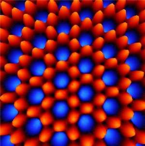 A two-dimensional "electronic metamaterial" is generated by supramolecular selfassembly on a metal surface. The periodic influence of the porous molecular network on the otherwise free-electron-like surface state results in the formation of an electronic band.
The interdisciplinary team of physicists and chemists have developed a substance which, after heating on a copper surface, exhibits a two dimensional network with nanometer sized pores. The interaction of this network with the existing electron gas on the metal surface leads to the following effect: the electrons underneath the network are pushed into the pores to form small bunches of electrons called quantum dots.
Great potential for materials research
By varying parameters such as the height and diameter of the pores the possibility arises to selectively tune the properties of the material. Further possibilities arise from the ability to fill the pores with different molecules. This allows direct access to the properties of the material which are dependent on the electronic structure, such as conductivity, reflectivity and surface catalysis properties. This will lead to the emergence of new materials with adjustable electronic properties.
The underlying physical mechanisms can best be understood by a comparison of the electron-gas with waves in water. Waves on a water surface are reflected by any obstacle they meet. If the obstacle on the surface in question resembles a honeycomb structure, standing waves are set up in each cell of the honeycomb. This then leads to a wave pattern representative of the honeycomb structure of the same size and shape. “Applying this analogy to the electron gas, we see that the interaction of the network structure with the electron gas on the metal surface confines the electrons giving rise to a characteristic electron wave structure of the new material.” says Stöhr.
These pore networks are good candidates for new meta-materials. These are man-made materials which, due to their period architecture, have specific optical and electronic properties not found in nature. These properties can be tuned by changing the properties of their component materials. In the case of pore networks, it is the electronic surface properties which can be tuned by careful selection of the nano-pores.
The University of Basel and the Paul Scherrer Institute are long-term partners of the Swiss Nanoscience Institute (SNI), which is also financed by the Canton of Aargau. The SNI also includes both the Nationaler Forschungsschwerpunkt Nanowissenschaften which was founded in 2001, and the Argovia-Netzwerk, founded in 2006 and also financed by the Canton of Aargau. A key partner in this project was the Swiss Light Source of the Paul Scherrer institute.