Aug 5 2009
Shinichi Shikata, Hideyuki Watanabe and others of the Device R+D Team, the Diamond Research Center of the National Institute of Advanced Industrial Science and Technology (AIST) have succeeded in the vapor-phase synthesis of a stack of nanometer-scale thin films of diamond using carbon isotopes 12C and 13C, which differ in mass. Electrons and holes were confined to a single material for the first time using the diamond stack.
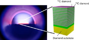 A view into the microwave plasma-assisted CVD reactor and a schematic illustration of the structure after deposition of diamond film
Among all available materials, diamond has the optimal characteristics with respect to hardness, thermal conductivity, light transmission wavelength range, and chemical stability. Furthermore, as a semiconducting material, diamond shows excellent characteristics in terms of breakdown electric field and carrier mobility, suggesting prospective application to electrochemical and semiconductor devices, in addition to mechanical and optical applications. As a semiconductor, diamond appears to have a promising future in high-performance materials for power devices and quantum computers. Studies are still underway because the aspects of diamond as a semiconducting material have not yet been fully explored.
In this study, diamonds were synthesized using a microwave plasma-assisted chemical vapour deposition (CVD) method, from methane (CH4) gases containing only 12C or 13C carbon isotopes. A super lattice structured diamond was prepared by alternately depositing 25 diamond layers, each containing only 12C or 13C, with thickness of 30 nm. The layered diamond was irradiated with an electron beam and the electron-hole recombination was measured. It was found that recombination occurred only in the 12C-containing diamond layers, indicating that electrons and holes were confined to 12C layers. So far, the confinement of electrons and holes has been reported only with a combination of different materials (GaAs/AlGaAs, InGaAs/InP, etc.); this study reports the first success with a single material. The result makes structural design of a single material using the semiconductor band-gap engineering possible, and it offers an effective means for developing ultrafast devices and quantum functional devices.
The result of the study appears in the electronic version of the American journal "Science" on June 12, 2009.