Imec and its partners have successfully fabricated Au-free, Si-processing compatible GaN power devices on a 6 inch Si wafer. This result is a milestone in imec’s industrial affiliation program (IIAP) on GaN power and light-emitting (LED) devices that targets cost reduction as one of the main objectives.
Fabrication of the Au-free Si-processing compatible GaN power device follows an earlier transfer of imec’s process flow from its III-V processing lab on 4 inch Si, to a 6 inch Si processing line. The transfer included the development of Au-free ohmic contacts and gate structures. While on 4 inch, the metal patterning was done using contact lithography and lift-off, the 6 inch process uses I-line lithography and metal dry etch.
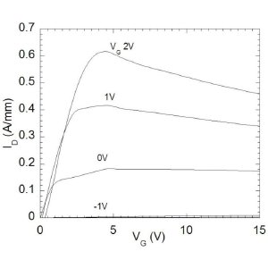
 I-V characteristic of the GaN power device showing the viability of the Au-free Si-processing compatible process flow
The availability of a Au-free Si-processing compatible process flow for fabricating GaN power devices is an important milestone for imec’s IIAP on GaN power and LED devices. In this program, cost reduction is one of the key objectives. In order to achieve this, the program targets growth of GaN/AlGaN layers on top of Si substrates, which allows for an upscaling of the wafer size towards 8 inch substrates. The increase of the wafer size has been a decisive factor in the reduction of chip cost in Si processing as more chips are available on larger area substrates. GaN power and LED devices could not follow this increase as the competing SiC or sapphire substrates are not becoming available at large wafer diameters. Furthermore, the program targets a process flow that is compatible with a Si processing line. The use of high-throughput high-capacity 200mm Si processing fabs is therefore a second element in the cost reduction. But to achieve this compatibility, the processes cannot use incompatible materials, especially Au for ohmic contacts and gate structures.
The GaN materials system offers the possibility to fabricate high-electron-mobility transistors (HEMTs) that offer a competitive advantage compared to Si power devices. GaN is a wide bandgap material, and as such an isolator. When an AlN or AlGaN layer(s) is processed on top of a GaN channel, a hetero-junction structure is formed, with a large two-dimensional electron gas (2DEG) at the hetero-junction. Because dopant impurities are absent and the current does not flow at the surface but at the hetero-junction, the high concentration 2DEG has a high mobility allowing for fast switching. Together with the high bandgap of the material, a competitive trade-off between breakdown voltage and on-resistance is achieved. The resulting transistors have low switching losses, high voltage capability, and a high operating frequency. The latter allows for a smaller form factor of systems that use these switching components, such as power invertors and DC/DC convertors. The transformers, inductors and capacitors can indeed be made substantially smaller at these high frequencies.
Currently, further optimization of the 6 inch process flow is underway. The 6 inch facility used for this development is the MiPlaza 6 inch development fab in Eindhoven, The Netherlands, and the project is executed by a joint imec/MiPlaza team. In addition, a new reactor for GaN epitaxy on 8 inch Si has been acquired, and the challenging epitaxy process on 8 inch is being developed. When GaN on 8 inch Si substrates become available, the learnings on 6 inch will be transferred to imec’s 8 inch Si processing line.
Since imec launched the IIAP on GaN-on-Si technology in July 2009, six industrial partners including equipment vendors, substrate suppliers and IDMs have already joined the program.