Feb 5 2011
Versatilis LLC, a high technology development Company based here, announced today it has developed a method for significantly increasing the performance of the organic semiconducting inks used for printing electronic circuits.
Working with research partner Lehigh University under a Small Business Technology Transfer (STTR) grant from the Office of Naval Research, Versatilis showed polymer transistors with 5-fold improvement over what could be otherwise achieved in such devices without incorporating its technology.
 Semiconductor Device with Embedded Percolating Network of Nanoparticles
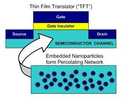
Electronic devices made of organic or amorphous inorganic semiconductor materials, especially those made of “printable” semiconductor inks, have poor performance when compared to conventional silicon electronics. This is largely due to the very low intrinsic ability of such semiconductors to transport electrical charges, a problem that severely limits, for example, the appeal of printed electronics for higher end applications. Versatilis’ technology involves mixing conductive nano- or micro-particles into the semiconductor host material to form so-called percolating networks of dispersed particles. Such networks of embedded conductive particles enable electrical charges to take “shortcuts” effectively shortening their travel path, and dramatically improving device performance such as switching speed and other parameters.
The effect had been previously demonstrated using carbon nanotubes to form percolating networks in a so-called “pick-up stick” transistor, but carbon nanotubes have presented a variety of challenges, all of which are circumvented by Versatilis’ technique using particles.
Versatilis demonstrated a number of thin film transistors made with such embedded conductive particle based percolating networks and has been awarded the first broad patent (US 7,879,678) of several still pending. “We are delighted to introduce this technology to the industry, and are discussing a number of exciting follow-on projects,” said Ajay Jain, Versatilis CTO and the principal inventor of the technology, adding that existing printing technologies can be used, for example in a roll to roll manufacturing scheme since feature sizes can be larger for equivalent device performance.
The technique can be used at high production rates in such a manner, as well as on wafers in batch mode. As a complement to this technology, Versatilis had also acquired in November last year the assets of Nanometrix, Inc., which included a novel technology for depositing ultra-thin, nano-scale coatings as well as monolayers of particles. “We can offer a combined technology solution with a tool that facilitates the laying down of organic semiconductor inks with embedded particles as well as semiconducting particles including so-called hybrid inks at high rates,” said George Powch, Versatilis CEO.
Source: http://www.versatls.com/