Feb 11 2011
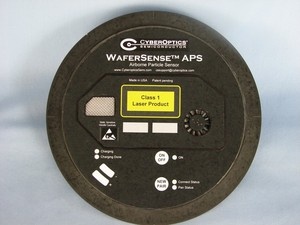
After a year of beta testing and product analysis, CyberOptics Semiconductor, Inc. has released the WaferSense® Airborne Particle Sensor (APS) for wafer processing equipment to the semiconductor market.
The only semiconductor sensor of its kind to identify particle sources in tools, the Airborne Particle Sensor moves through semiconductor process equipment and automation material handing systems to monitor airborne particles, reporting information in real-time to allow engineers to efficiently validate wafer contamination. With a wafer-like shape compatible with existing automation and wireless communication providing real-time data, the Airborne Particle Sensor speeds tool qualification and release to production. APS reduces time locating particle sources.
 WaferSense® Airborne Particle Sensor
With real-time views of particle conditions, process engineers can address specific trouble spots and be better prepared to pass particle qualifications on the very first attempt. The metrology device can also be used to establish a baseline and to ensure operations continue on this baseline as part of preventive maintenance.
“In the past, it could take engineers hours to determine where a particle event is occurring or if a particle related PM or qualification was done correctly to release tools for manufacturing,” stated Craig Ramsey, Ph.D, CyberOptics Semiconductor General Manager. “The Airborne Particle Sensor represents a significant change in particle-detection methodology, enabling engineers to really monitor and control contaminations in their tools and protect die yield – with real-time views of particle conditions to address areas of concern instead of the whole tool.”
How it Works
The Airborne Particle Sensor uses a fan to pull non-corrosive gas or air through a channel as a laser illuminates the air/gas stream while particles scatter light onto the sensors photodiode. Compatible with front-ends, coater/developer tracks, deposition and etch equipment, the APS has the ability to detect particles as small as 0.1 um. The automation-friendly semiconductor sensor doesn't require engineers to open chambers or expose ultra-clean process areas to the environment. The sensor can detect particles in real-time without opening the tool.
Using the Airborne Particle Sensor’s companion software, ParticleView™ and ParticleReview™, fab engineers can collect and display particle data wirelessly to see the effect of adjustments in real time, speeding equipment qualification and setup. Particle data can be recorded to compare past to present operations as well as one tool to another to conduct machine-to-machine trend analysis of particle conditions and to establish process control and conduct process improvement.
Source: http://www.cyberopticssemi.com/