The semiconductor industry is working on the development of cost-effective technique to etch microscopic features onto microchips. The ultimate solution could be the extreme-ultraviolet (EUV) lithography technique that utilizes very-short-wavelength light to etch features that are four folds finer when compared to existing microchips. However, the industry requires huge investment to overcome the physics, chemistry and engineering challenges.
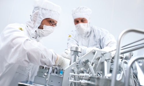 ASML devices make EUV light by turning tin into plasma. Credit: ASML
Microchip manufacturer, Intel made an announcement on July 9, 2012, according to which the company plans to make a $4.1 billion investment in ASML, a lithography equipment provider based in Veldhoven, the Netherlands. One-fourth of the investment will be used for research and advancement of EUV equipment.
Smallest features on present chips are 22 nm across and are etched utilizing deep ultraviolet light with around 193 nm wavelength. However, this process has its own challenges. Shortening the wavelength is the only method to etch smaller features and a 13.5 nm wavelength must enable microchip companies to create features £5 nm. However, this drastic shortening will entail redefining of the light source, masks, photoresists and optics behind lithography systems. Most components of the process are available for prime time; however, problems are still encountered with the light source.
The process must occur in a vacuum because light with short wavelengths is absorbed by all materials, including air. Since traditional lenses and mirrors cannot guide light, optics maker Carl Zeiss has to develop alternative designs. However, even these special mirrors made of 80 alternating atomically smooth silicon and molybdenum layers absorb a high amount of EUV light, hence the light must have high brightness, according to Jos Benschop, ASML's Senior Vice President for technology.
The power of the EUV source is crucial to reduce costs because curing of photoresist will take more time when the light is dimmer. Benschop informed that commercial systems must be able to achieve 200 W and pattern no less than 100 wafers per hour. For this purpose, ASML is working with Cymer and XTREME Technologies. For example, Cymer is perfecting a system that utilizes a 20-kW laser to blast tin droplets into a 500,000-degree plasma that releases EUV light.
ASML is likely to achieve its goal in a few years. Intel stated that existing technology can be utilized for two more generations of microchips with the integration high-cost patterning steps and through the purchase of additional lithography tools. While ASML is working on the development of first commercial EUV lithography tools, in the meantime, Intel plans to shift to 450-mm-wide wafers from present 300-mm-wide silicon wafers for EUV lithography, thus posing another challenge to ASML. This move could increase the count of simultaneous patterning of circuits by two fold. However, ASML has to devise a new production tool for this purpose. Intel wants this new tool by 2016.