AIXTRON SE today announced that the University of Cincinnati (UC), USA, has ordered a new BM system to further develop its longstanding research into carbon nanotubes (CNT). The system set up for handling 4-inch substrates has been installed at Nanoworld Laboratories – an interdepartmental research facility that includes faculties from Mechanical Engineering, Materials Engineering, Chemistry, Physics and Medical School, and is directed by Professors Vesselin Shanov and Mark Schulz.
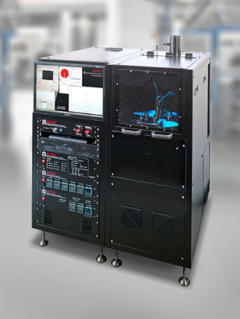
Professor Shanov, comments: “The BM system possesses many advanced features, such as rapid heating, vertical reactor with shower head, and plasma operation. These features allow us to control the growth of carbon nanotubes and graphene. We will be using the BM system to grow CNT for use in fiber formation, devices and composites, and graphene for advanced energy and space applications.
"We went for an AIXTRON product because the company has shown considerable expertise in deposition of carbon nanomaterials, provides dedicated support for our process development through its laboratory, and has demonstrated that its reactor technology is truly scalable to meet future production needs for these applications.”
The Nanoworld facility develops a wide range of smart materials, sensors and devices by combining nanotechnology, biomedical, composites and smart structures expertise from across the science-engineering spectrum.
Nanoworld also offers an important interdisciplinary experimental-theoretical learning environment for undergraduate through PhD level students.
About AIXTRON
AIXTRON AG is a leading provider of deposition equipment to the semiconductor industry. The Company's technology solutions are used by a diverse range of customers worldwide to build advanced components for electronic and opto-electronic applications based on compound, silicon, or organic semiconductor materials and more recently carbon nanostructures.
Such components are used in display technology, signal and lighting technology, fiber communication networks, wireless and cell telephony applications, optical and electronic data storage, computer technology as well as a wide range of other high-tech applications.