Researchers at Aalto University have developed a new method to implement different types of nanowires side-by-side into a single array on a single substrate. The new technique makes it possible to use different semiconductor materials for the different types of nanowires.
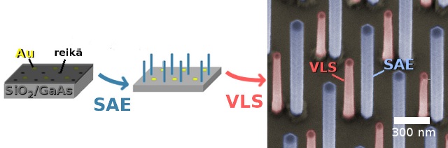 Initially the substrate is prepared by depositing Au nanoparticles on it and covering it with a hole-patterned oxide. The first nanowires grow from these holes and after the oxide is removed, the other type of nanowires are grown via the deposited nanoparticles. The resulting dual-type array is presented on the electron micrograph on the right. (Credit: Aalto University)
'We have succeeded in combining nanowires grown by the VLS (vapor-liquid-solid) and SAE (selective-area epitaxy) techniques onto the same platform. The difference compared with studies conducted previously on the same topic is that in the dual-type array the different materials do not grow in the same nanowire, but rather as separate wires on the same substrate', says Docent Teppo Huhtio.
The research results were published in the Nano Letters journal on 5 February 2015.
Several applications
The new fabrication process has many phases. First, gold nanoparticles are spread on a substrate. Next, the substrate is coated with silicon oxide, into which small holes are then patterned using electron beam lithography. In the first step of growth, (SAE), nanowires grow from where the holes are located, after which the silicon oxide is removed. In the second phase different types of nanowires are grown with the help of the gold nanoparticles (VLS). The researchers used metalorganic vapor phase epitaxy reactor in which the starting materials decompose at a high temperature, forming semiconductor compounds on the substrate.
'In this way we managed to combine two growth methods into the same process', says doctoral candidate Joona-Pekko Kakko.
'We noticed in optical reflection measurements that light couples better to this kind of combination structure. For instance, a solar cell has less reflection and better absorption of light', Huhtio adds.
In addition to solar cells and LEDs, the researchers also see good applications in thermoelectric generators. Further processing for component applications has already begun.
Nanowires are being intensely researched, because semiconductor components that are currently in use need to be made smaller and more cost-effective. The nanowires made out of semiconductor materials are typically 1-10 micrometres in length, with diameters of 5-100 nanometres.
The research was conducted at the Aalto University School of Electrical Engineering. The research received funding from Aalto University's Aalto Energy Efficiency Research Programme AEF.