Mar 27 2015
Brown University researchers have developed a new method of producing new 2D multilayered graphene-like semiconductor materials in a variety of shapes and orientations using silicon telluride.
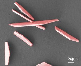 A new process for an old standby - by adjusting the fabrication technique, researchers can make different semiconductor structures, including nanoplates that lie flat or stand upright. (Credit - Koski lab/Brown University)
The research, published in Nanoletters, demonstrates the process of creating nanoplates and nanoribbons using a silicon telluride compound. The p-type semiconductor materials are produced in their purest form, and they could be employed in optical and electronic devices. As their layered structure are capable of taking up magnesium and lithium, the materials also hold promise in battery applications.
“Silicon-based compounds are the backbone of modern electronics processing. Silicon telluride is in that family of compounds, and we’ve shown a totally new method for using it to make layered, two-dimensional nanomaterials ” said Kristie Koski, assistant professor of chemistry at Brown University, who led the work.
Koski, along with her co-workers, produced the new materials in a tube furnace using vapor deposition technique. Upon heating, silicon and tellurium vaporize and react to form a precursor compound, which is then deposited on a substrate using an argon carrier gas. The resulting precursor compound is then used to grow the silicon telluride.
Using various substrate treatments and adjusting the furnace temperature, it is possible to form different structures. By adjusting these parameters, the researchers generated nanoribbons of nearly 10 µm length and width of between 20 and 1000 nm. They also developed flat nanoplates over the surface.
“We see the standing plates a lot. They’re half hexagons sitting upright on the substrate. They look a little like a graveyard,” Koski said.
Each shape thus produced has a crystalline structure with different orientation and properties, which enable diverse applications.
The researchers also proved that the material can doped with various substrates. Doping allows the introduction of small impurities to alter the material’s electrical properties. They also showed the doping of silicon telluride with aluminum on a sapphire substrate. This process may transform the material from a p-type semiconductor to an n-type.
Koski said that the materials remain unstable outside the environment. “What we can do is oxidize the silicon telluride and then bake off the tellurium, leaving a coating of silicon oxide. That coating protects it and it stays pretty stable,” she added.
The team has plans to further analyze the electronic and optical properties of the material. “We think this is a good candidate for bringing the properties of 2-D materials into the realm of electronics,” Koski said.
The co-authors of the paper include undergraduates Frank Chung and Jeffrey Commons, graduate student Mengjing Wang, and postdoctoral researcher Sean Keuleyan.