Nanoscale defects are enormously important in shaping the electrical, optical, and mechanical properties of a material. For example, a defect may donate charge or scatter electrons moving from one point to another. However, observing individual defects in bulk insulators, a ubiquitous and essential component to almost all devices, has remained elusive: it’s far easier to image the detailed electrical structure of conductors than insulators.
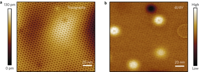 (a) STM topographic image of a clean graphene/BN area (b) dI/dV map acquired simultaneously with (a) exhibits new features including bright dots, a dark dot and a ring.
Now, Berkeley Lab researchers have demonstrated a new method that can be applied to study individual defects in a widely used bulk insulating material, hexagonal boron nitride (h-BN), by employing scanning tunneling microscopy (STM).
“Normally, STM is used to study conductors and cannot be used to study bulk insulators, since electrical current does not typically flow through an insulator,” explains Mike Crommie, physicist at Berkeley Lab’s Materials Sciences Division and professor at UC Berkeley, in whose lab this work was conducted. His team overcame this obstacle by capping the h-BN with a single sheet of graphene.
“This permits us to visualize the charged defects embedded in the underlying BN crystal,” Crommie says. “Essentially, we use graphene as a window to look into the insulator.”
Adds Jairo Velasco Jr, also a member of the Materials Sciences Division and a lead co-author of this work, “In contrast to previous studies that were limited to spatially averaging defect behavior, our experiment visualizes individual point defects embedded inside a BN crystal with nanoscale precision. The STM allows details of a defect’s electronic properties to be extracted by directly detecting how electrons in graphene respond to the defect in the underlying bulk insulator.”
Graphene synthesis and characterization, performed at the Molecular Foundry, a DOE Office of Science User Facility, aided the researchers in visualizing and even manipulating individual defects in the underlying bulk BN insulator. New features in STM topographic and energy-dependent electron density images included randomly distributed dots and rings of varying intensities.
“We discovered that it is possible to selectively manipulate the charge states of individual BN defects by applying voltage pulses with our STM tip,” Velasco says.
The new technique provides a valuable tool for the many scientists in the 2D materials community who use h-BN. It may also be used to study other insulators such as diamond with nitrogen-vacancy centers—a popular system for nanoscale sensing.
Crommie is the corresponding author on a paper describing this research in the journal Nature Nanotechnology. The paper is entitled “Characterization and manipulation of individual defects in insulating hexagonal boron nitride using scanning tunnelling microscopy.” Co-authors are Dillon Wong, Jairo Velasco Jr, Long Ju, Juwon Lee, Salman Kahn, Hsin-Zon Tsai, Chad Germany, Takashi Taniguchi, Kenji Watanabe, Alex Zettl, and Feng Wang .
This research was funded by the DOE Office of Science.