Nov 17 2017
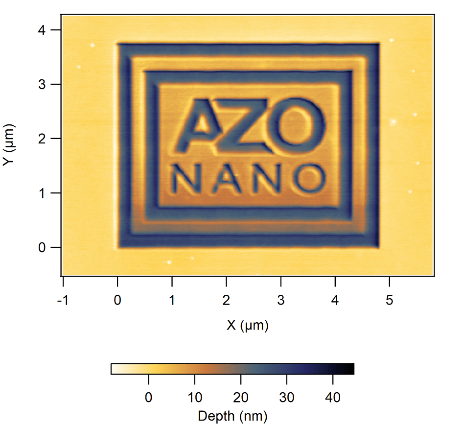
Image Credits: AXT
Nanofabrication or the process of producing structures with nanoscale features is gaining in importance, specifically in the field of microelectronics. New technologies such as thermal scanning probe lithography (t-SPL), originally developed by IBM Research Laboratories and recently commercialized by SwissLitho are proving to be viable alternatives the mainstay, EBL.
The Nanofrazor Explore
The Nanofrazor Explore is designed specifically for nanofabrication of patterns and structures at the nanoscale. The geometries are produced quickly in high resolution with this instrument, which offers unparalleled accuracy and precision.
The Nanofrazor t-SPL system used a heated AFM tip to vaporize the photoresist coating on a semiconductor substrate to yield high precision 3D nanopatterns with accuracy better than 10 nm in X and Y and better than 1 nm in the Z-direction. Furthermore, the ability to carry out in situ AFM allows the user to image the generated structure with no need for developing or dissolving the photoresist, thus speeding up the prototyping process.
The image above produced for the AZoNano.com team using the Nanofrazor, located in Switzerland remotely operated from Australia by Dr. Cameron Chai of AXT. The ability to operate the instrument remotely enables increased levels of productivity, through unattended operation and operation from various locations and time zones.
Thermal Scanning Probe Lithography vs E-Beam Lithography
As we mentioned previously t-SPL is becoming a feasible alternative to the traditional EBL method, due to several advantages over this technique.
t-SPL allows in situ inspection to be performed, with <1 nm vertical resolution, and 3D nanolithography with <2 nm vertical accuracy; both of which cannot be achieved with EBL.
Closed-loop lithography, correction overlay, correlation stitching, and chemical patterning are also realized with t-SPL, creating new application opportunities.
t-SPL is also a more efficient technique compared to EBL due to the lower energy consumption, maintenance costs, and footprint.
Applications
The Nanofrazor Explore can be used for a wide array of nanofabrication applications, including nanophotonics, where photonic crystals, cavities, and waveguides can be fabricated with low roughness.
The instrument also has the ability to create novel nanoelectronics such as nanowire and quantum devices, that use a precise overlay. Studies on spintronics and artificial spin ice can be aided with the use of the Nanofrazor Explore, with the fabrication of smaller magnetic structures.