Jul 10 2018
Atoms are the constituents of all matter and are too small to be observed without powerful advanced instruments such as electron microscopes. The same electrons forming images of atomic structures can even be used to move atoms in materials.
At present, this method of single-atom manipulation, introduced by scientists from the University of Vienna, has been able to accomplish almost perfect control over the movement of individual silicon impurity atoms in the lattice of graphene, the two-dimensional sheet of carbon. The outcomes of the study have been published in Nano Letters, a scientific journal.
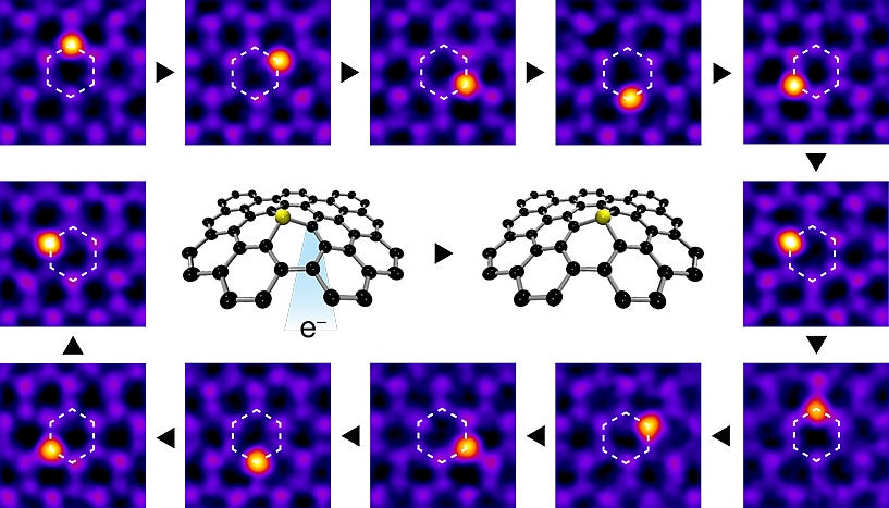 An electron beam focused on a carbon atom next to a silicon impurity atom can controllably make it jump to where the beam was placed. Step by step, this allows the silicon to be moved with atomic precision around a hexagonal path. (Image credit: CC-BY, Toma Susi/University of Vienna)
As an outstanding achievement in nanotechnology, from the late 1980s, the scanning tunneling microscope has been able to move atoms over surfaces, and to date, it has been the only technology with the ability to move individual atoms in a controlled way.
At present, the scanning transmission electron microscope (STEM) has gained the potential to reliably focus an electron beam with sub-atomic precision, enabling researchers to directly observe each atom in two-dimensional materials such as graphene, and also to target single atoms using the beam. Each electron has a tiny possibility of being scattered back from a nucleus, providing it a kick in the opposite direction.
Adding to the studies reported in the last few years, a research group from the University of Vienna, headed by Toma Susi, has now employed the sophisticated electron microscope Nion UltraSTEM100 to move single silicon atoms in graphene with absolutely atomic precision. Even with manual operation, the realized movement rate is already on par with the state-of-the-art in any atomically precise method.
The control we are able to achieve by essentially directing the electron beam by hand is already remarkable, but we have further taken the first steps towards automation by detecting the jumps in real time.
Toma Susi, University of Vienna
The new outcomes also enhance theoretical models of the process by including simulations by colleagues in Belgium and Norway.
The researchers recorded a total of almost 300 controlled jumps. In addition to elongated paths or moving around a single hexagon formed of carbon atoms in graphene, it would be possible to move a silicon impurity backward and forward between two adjacent lattice sites separated by one tenth-billionth of a meter, similar to flipping an atomic-sized switch. In general, this can be used to store one bit of information at density like never before. Dr Susi concluded saying, “Your computer or cellphone will not have atomic memories anytime soon, but graphene impurity atoms do seem to have potential as bits near the limits of what is physically possible.”
The European Research Council (ERC) and the Austrian Science Fund (FWF) provided the main funding for this study.