Aug 29 2018
Semiconducting heterostructures have been vital to the advancement of electronics and opto-electronics. Various applications in the terahertz and infrared frequency range make use of transitions, known as intersubband transitions, between quantized states in semiconductor quantum wells.
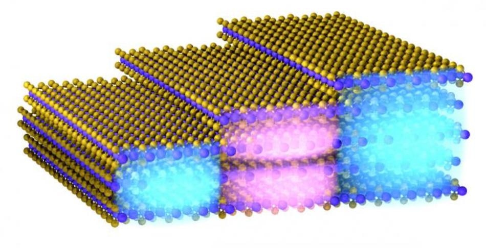 Schematic illustration of charge carriers confined within a TMD flake comprising different thicknesses. Charge carriers in the ground state (blue) can be excited upon resonant light excitation to a higher state (pink). (Image credit: ICFO/Fabien Vialla)
Such intraband transitions demonstrate remarkably large oscillator strengths, close to unity. The discovery of these transitions in III-V semiconductor heterostructures had a large influence on the field of condensed matter physics and initiated the development of quantum well infrared photodetectors and also quantum cascade lasers.
In general, quantum wells of the highest quality are produced by employing molecular beam epitaxy (sequential growth of crystalline layers), which is a well-established method. Yet, it has two major drawbacks: It requires lattice-matching, thereby constraining the freedom in choosing the materials, and the thermal growth leads to atomic diffusion and increases interface roughness.
Since 2D materials naturally form a quantum well that has atomically sharp interfaces, they have the ability to overcome these drawbacks. They offer atomically sharp and defect-free interfaces, thereby allowing the formation of perfect quantum well, free of diffusive inhomogeneities. They eliminated the need for epitaxial growth on a matching substrate and hence can be easily isolated and coupled to other electronic systems such as optical or Si CMOS systems such as waveguides and cavities.
Astonishingly, theoretical or experimental analysis of intersubband transitions in few-layer 2D materials has never been performed. As a result, in a research recently reported in the Nature Nanotechnology journal, ICFO researchers Peter Schmidt, Fabien Vialla, Mathieu Massicotte, Klaas-Jan Tielrooij, and Gabriele Navickaite, headed by ICREA Professor at ICFO Frank Koppens, in collaboration with the Institut Lumière Matière–CNRS, Technical University of Denmark, Max Planck Institute for the Structure and Dynamics of Matter, CIC nanoGUNE, and the National Graphene Institute, report on the first theoretical calculations and first experimental observation of intersubband transitions in quantum wells of few-layer semiconducting 2D materials (TMDs).
In their experiment, the group of scientists applied scattering scanning near-field optical microscopy (s-SNOM) as a novel strategy for performing spectral absorption measurements with a spatial resolution less than 20 nm. They exfoliated TMDs consisting of terraces of different layer thicknesses over lateral sizes of around a few microns. The researchers directly observed the intersubband resonances for these distinctive quantum well thicknesses inside a single device. They also tuned the charge carrier density in an electrostatic manner and illustrated intersubband absorption in both the conduction and valence bands. Detailed theoretical calculations were performed to complement and support these observations, which revealed non-local and many-body effects.
The outcomes of this research open the door for an unexplored area in this new category of materials and provide a preview of the physics and technology facilitated by intersubband transitions in 2D materials, such as infrared sources, detectors, and lasers with the capability for compact integration with Si CMOS.