A p-n junction configuration is created by doping a semiconductor crystal with p-type dopants in one region and with n-type dopants in another region. p-n junctions are the basic building blocks of solar cells, light emitting diodes, and other semiconductor transistors.
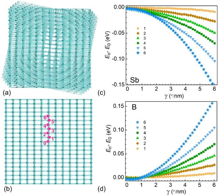 Illustration of the relative formation energy as function of twist rate γ of doped Si nanowire for Sb and B dopants at different atomic sites. The strain-free and twisted Si nanowires are shown at the axial view. (Image credit: Science China Press)
In addition, p-n junctions in nano-structures are anticipated to be the basic units of next-generation nano-devices. However, the strong attraction between the n-type dopants and p-type dopants cause them to form neutral pairs. Consequently, the p-n junction fails. In order to avoid such attraction between p-type dopants and n-type dopants, heterostructures are set up, in which one semiconductor material is doped with p-type dopants while the other is doped with n-type dopants, and the interface between two different semiconductor materials serves as an energy barrier between p-type dopants and n-type dopants.
In fact, the usage of heterostructures represents a model for the material design of the p-n junction. It is now possible to form comparable p-n junction configurations for nanowire heterostructures, for example, co-axial core-shell nanowires. However, nanowire heterostructures have a number of restrictions. For instance, the production of core-shell nanowires typically involves a two-step process, which leads to additional costs. Usually, the shell of the acquired nanowire heterostructure is polycrystalline. Such a defect is made worse with the transport of carriers. Additionally, the interface between the shell and core also introduces detrimental deep centers that greatly obstruct the device efficiency.
Is it possible to create p-n junctions with single crystalline nanowires? Honestly, the answer will be “No” if one thinks the issue instinctively. Certainly, just like the bulk, p-type dopants and n-type dopants in a codoped single crystalline nanowire also experience strong Coulomb attraction. How is it possible to overcome such attraction without an interface? It needs an effective modulation/control of the spatial occupation regions, which means the spatial distribution of dopants.
Indeed, this is one of the long-standing and basic problems concerning doping in semiconductors. From the perspective of materials engineering, this can be ascribed to the failure of traditional methods such as hydrostatic, uniaxial, and biaxial stresses on the modulation of the spatial distribution of dopants. However, all these discussed distortions are uniform, can some inhomogeneous ones like twisting be employed? Actually, twisting of structures signifies a focus of recent condensed matter physics research in low dimensions.
In a new paper reported in National Science Review, a team of researchers from Beijing Normal University, the Chinse University of Hong Kong, and Beijing Computational Science Research Center describe their theoretical advances of codoped Si nanowire under twisting. They use microscopic simulations based on the generalized Bloch theorem as well as analytical modeling based on the bond orbital theory to carry out the research and uncover the physics behind.
Fascinatingly, twisting has a considerable effect on the distribution of dopants in nanowires. As shown in the figure, a dopant of larger atomic size(Such as Sb) in a twisted Si nanowire has lower formation energy if it occupies an atomic site nearer to nanowire surface. In contrast, a dopant of smaller atomic size (Such as B) has lower formation energy if it occupies an atomic site around the nanowire core.
As per their estimations, n-type and p-type dopants can be separated in the codoped nanowire with appropriate selections of codoping pairs, for example, B and Sb. A bond orbital analysis shows that the effective modulation is promoted by the twist-induced inhomogeneous shear strain along nanowire radial dimension. These findings are completely backed by generalized Bloch theorem simulations based on density-functional tight-binding.
This new approach primarily makes the manufacturing process easy and decreases manufacturing costs. If the twisting is applied during the working mode of the device, the recombination of various types of dopants is greatly suppressed. The recombination is still difficult even if the twisting is eliminated while the device is in working mode because of the restricted diffusion.
This study was funded by the National Natural Science Foundation of China, Beijing Normal University, HKRGC funding, and the Chinese University of Hong Kong.