A study recently published in the journal ACS Nano sheds light on the creation of a pyrolyzed semiconductive cellulose nanofiber paper (CNP) with a three-dimensional (3D) network configuration.
Study: Laser-Driven Bubble Printing of Plasmonic Nanoparticle Assemblies onto Nonplasmonic Substrates. Image Credit: GiroScience/Shutterstock.com
The Logic Behind Creating a Nano-Micro-Macro Trans-Scale 3D Network
Modifying three-dimensional (3D) network frameworks at macro-, micro-, and nanoscales is a viable technique for creating material systems with exceptional properties and capabilities.
At the micro- and nanoscale levels, three-dimensional network topologies offer remarkable features such as great permeability and big surface areas, which are critical for separation as well as adsorptive, sensory, and biological purposes.
A macroscopic architecture of the nano–microstructures with a three-dimensional matrix is necessary to detect such features in sizable items for macroscale uses. Macroscopic structures with certain shapes may have intriguing mechanical features such as high compressibility for microscale pressure detection and elasticity for efficient light-catching and dissipation of heat.
The nano–micro–macro trans-scale architecture of 3D-network-containing frameworks is therefore critical for producing innovative substances with remarkable functionality and end-use diversity.
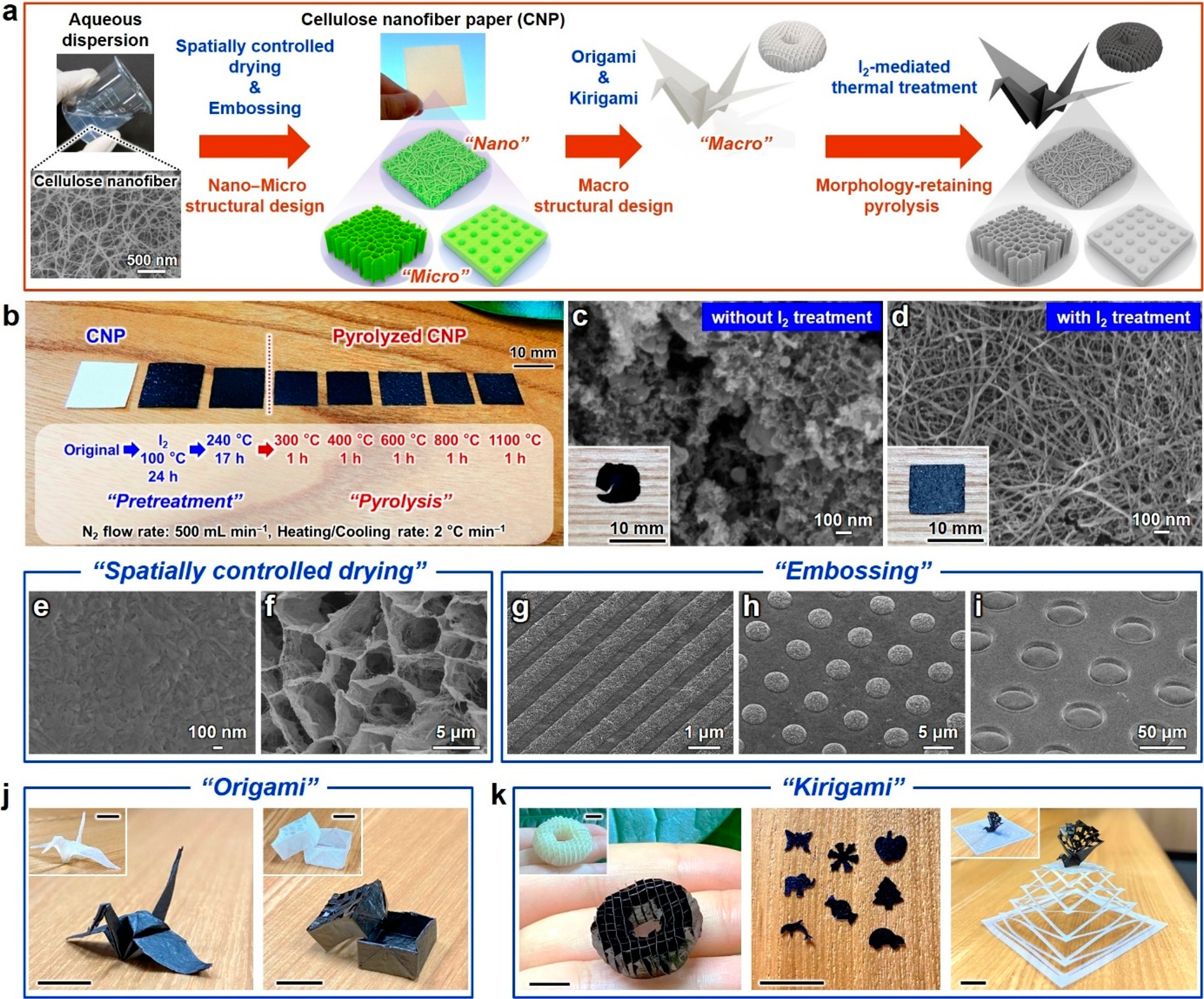
Figure 1. Nano–micro–macro trans-scale crafting and morphology-retaining pyrolysis of cellulose nanofiber paper (CNP). Schematics of (a) the nano–micro–macrostructural design and morphology-retaining pyrolysis of CNP and (b) the pretreatment and pyrolysis of CNP at different temperatures. Optical and field-emission scanning electron microscopy (FE-SEM) images of pyrolyzed CNP (c) without and (d) with I2 treatment. FE-SEM images of pyrolyzed CNP prepared using (e and f) spatially controlled drying and (g–i) microembossing. Optical images of the (j) origami- and (k) kirigami-processed CNPs before and after pyrolysis. White and black papers indicate the original and pyrolyzed CNPs, respectively. Scale bar in (j and k): 10 mm. Pyrolysis temperature: 600 °C (e–k) or 1100 °C (c and d).
3D Structured Framework of Semiconductive Nanomaterials
Three-dimensional modeling of semiconductive nanomaterials with adjustable electric conductance capabilities, employing synthesizing, self-assembly, and additive fabrication approaches have lately been documented for sophisticated electronic purposes.
The synthesis method yielded three-dimensional metallic oxides with nano–microscale porous architectures and three-dimensional organic semiconductors with a mean pore diameter of 0.4 nm. The self-assembly process enabled the creation of three-dimensional silicon or phosphorus-doped WO3 and MoO3 nanowires, as well as three-dimensional CdTe/Au nanoparticle architectures with nanosized pore diameters. Three-dimensional micro–macrostructured architectures of reduced graphene oxide (rGO), metallic oxides, and intermetallic complexes are possible using additive fabrication approaches such as 3D printing.
Despite these endeavors, the nano–micro–macro trans-scale model of three-dimensional semiconducting frameworks has only been realized on a few occasions. Material density regulation and doping with impurities were used to modify the electrical resistivity values of three-dimensional porous organic polymers, three-dimensional metallo–organic structures, and three-dimensional rGOs.
Adjusting the electric conductivity characteristics of semiconductors expands their utility and application to a wide range of devices. The usefulness of three-dimensional semiconducting structures, unfortunately, has been significantly hampered by the minimal tunability of their electric conductivity characteristics, since the electrical resistivity values of traditional three-dimensional semiconductive nanostructures can only be regulated to a small extent.
Both nano–micro–macro trans-scale modeling of three-dimensional semiconducting devices and broad control of their electrical characteristics thus remains difficult.
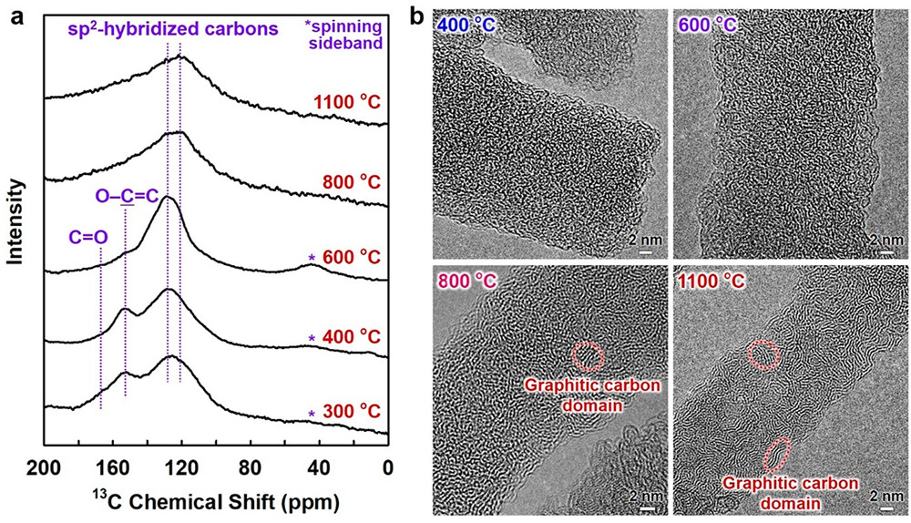
Figure 2. Molecular structures of pyrolyzed cellulose nanofiber. (a) Solid-state 13C nuclear magnetic resonance (NMR) spectra and (b) high-resolution transmission electron microscopy (HR-TEM) images for the cellulose nanofiber pyrolyzed at different temperatures.
Advantages of Using Cellulose Nanofiber Paper
Utilizing cellulose nanofibers (CNs) as nanoscale foundations, cellulose nanofiber paper (CNP) with three-dimensional nanofiber-network constructions with a diameter greater than 20 cm may be built.
CNP also exhibits mechanical qualities resembling those of paper, such as elasticity and pliability, indicating good prospects for structured model trans-scalability. Moreover, owing to the occurrence of sp3-hybridized carbons in molecules of cellulose, CNs possess a substantial electric resistance; hence, CNP is a good base material for the extensive tailoring of electric conductivity characteristics.
While high-temperature pyrolysis is a useful approach for reducing the electric resistivities of cellulose nanoparticles, the intrinsic shape of wood CNs deteriorates during pyrolysis, making the pyrolyzed CNP framework challenging to design.
Focus of the Study
In this work, a morphology-preserving and temperature-controlled progressive pyrolytic technique are used to enable three-dimensional nano–micro–macro trans-scale structured framework and electric resistivity adjustment of the pyrolyzed semiconducting CNP.
Important Takeaways
The nano–micro–macro trans-scale modelling of three-dimensional frameworks, with pore diameters, macroscopic morphology, and surface structure in the nanometer–centimeter range, and the extensive adjustability of electric resistivity are significant highlights of the pyrolyzed semiconducting CNP that outperforms hitherto documented three-dimensional semiconducting structures.
The pyrolyzed semiconducting CNP may therefore be customized in terms of architecture and functionality based on the intended purpose, enabling wide usability as a wearable water-vapor-selective detector and an electrode in enzymatic biofuel cells for energy production.
The chemical and electrical characteristics of the pyrolyzed semiconducting CNP might possibly be modified even more via altering its molecular architectures by utilizing different techniques such as heteroatomic doping.
This research might pave the way for modifying the function and applicability of semiconductive nanomaterials for a variety of electrical purposes. Since pyrolyzed semiconducting CNP may be made from common and plentiful biological materials, this technique has the potential to assist in the development of sustainable electronics.
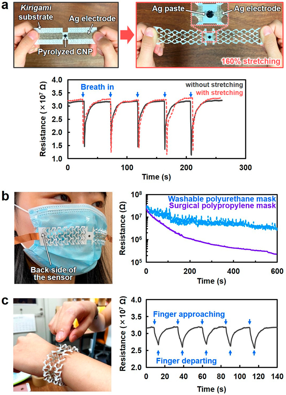
Figure 3. Stretchable and wearable sensor devices based on the pyrolyzed cellulose nanofiber paper (CNP) sensor and kirigami paper substrate. (a) Optical images of the sensor device and water vapor sensing in exhaled human breath before and after stretching, demonstrating the (b) monitoring of human exhalation-derived water vapor leaked from the face masks and (c) detection of skin moisture upon an approaching finger. The finger approaches close to ∼5 mm to the pyrolyzed CNP sensor and is held for 5 s, followed by departing away from the sensor.
Disclaimer: The views expressed here are those of the author expressed in their private capacity and do not necessarily represent the views of AZoM.com Limited T/A AZoNetwork the owner and operator of this website. This disclaimer forms part of the Terms and conditions of use of this website.
Source:
Koga, H., Nagashima, K. et al. (2022). Nanocellulose Paper Semiconductor with a 3D Network Structure and Its Nano–Micro–Macro Trans-Scale Design. ACS Nano. Available at: https://pubs.acs.org/doi/10.1021/acsnano.1c10728