Topological photonics witnessed significant advancements in the last few years. Due to topological protection, photonic devices have become more immune to scattering and robust against disorder. However, realizing topological nanophotonic devices are still considerably difficult owing to the challenges in nano-scale measurement, inherently weak magnetic response for natural materials in the near-infrared and visible range, and complexity in the fabrication process.
Synthetic dimensions can offer an insight into topological photonics beyond the geometric dimensions. Thus, synthetic dimensions can facilitate the fabrication of on-chip all-dielectric topological nanophotonic components, eliminating the limitations of magnetic materials.
Existing Limitations of Multi-frequency Topological Nanophotonic Devices
Multi-wavelength/multi-frequency devices are crucial components in nanophotonic chips used for applications with large information processing capacity. Among these multi-wavelength devices, the topological rainbow, a basic multi-frequency topological photonic device, can slow, separate, and trap topological photonic states of different frequencies into various positions.
However, this type of device has not been thoroughly investigated in studies until now. Additionally, effective methods for the direct measurement of multi-frequency topological photonic devices at the nanoscale are yet to be identified. Thus, these challenges restricted the application and development of the topological rainbow and different topological nanophotonic devices, such as topological temporary storage and topological router.
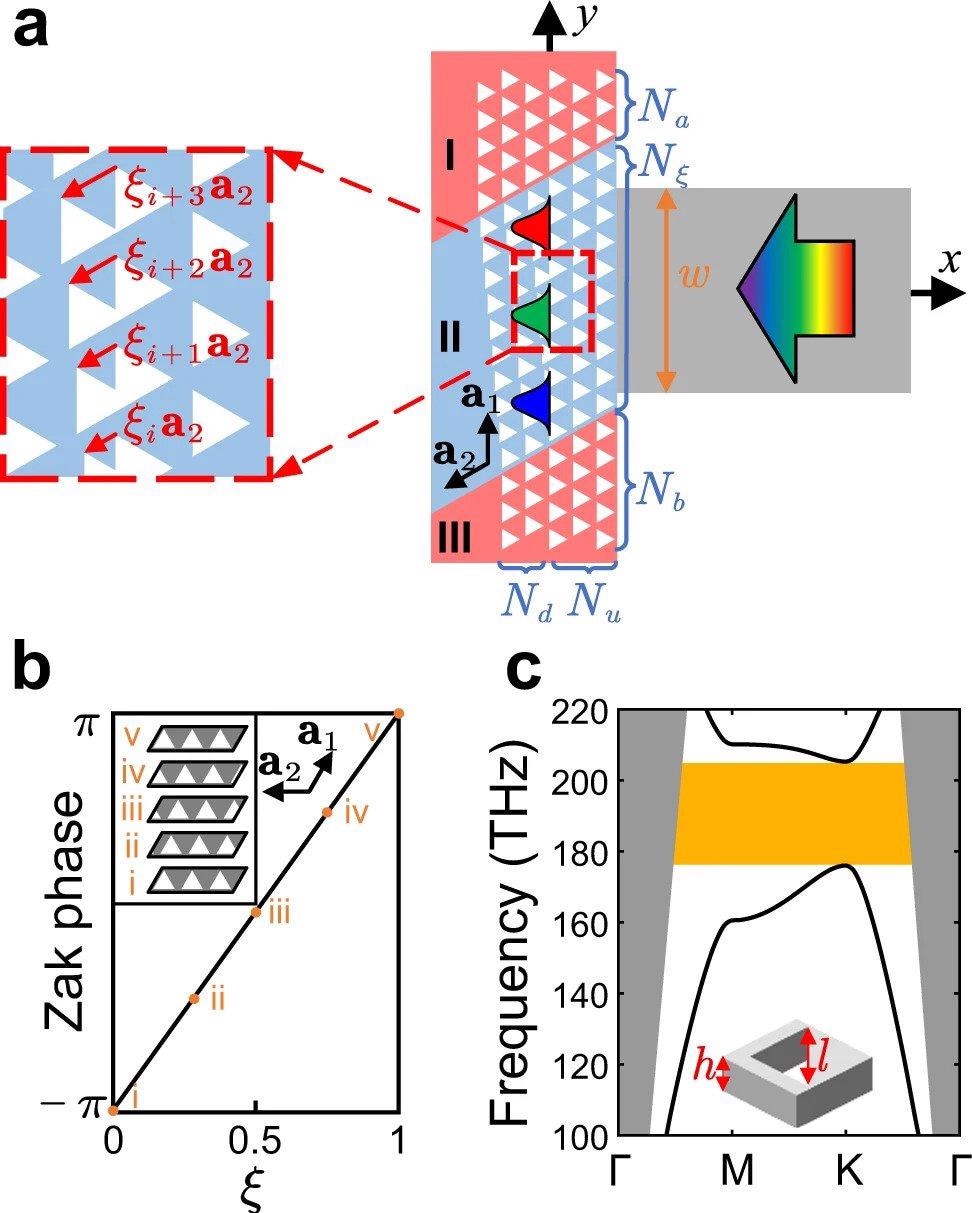
Schematic diagram of the topological rainbow configuration. a1, a2 denote the lattice vectors. The red and blue regions denote the barrier and dispersing regions, respectively. The displacement vector of ith layer is denoted by ξia2. Na, Nξ, Nb denote the number of layers of regions I, III along a1 direction, and Nu, Nd denote the number of layers of undeformed region and the deformed region in region II. Light is incident from the dielectric waveguide with a width w = 8 μm. b Evolution of Zak phases with parameter ξ. The inset shows the geometric structure for different ξs. c The TE-like bands of triangular hole structure with side length l = 0.75a and thickness h = 220 nm. The geometry of the unit cell is shown in the inset. © Lu, C., Hu, X., Wang, C. et al. (2022)
Novel Way to Fabricate Nanophotonic Topological Rainbow Device Based on Synthetic Dimension
In this study, researchers fabricated an on-chip nanophotonic topological rainbow device based on translational deformation freedom as a synthetic dimension, which represents an approach that is applicable for all wavelength ranges, dimensions, materials, symmetries, and optical lattice types.
In a topological rainbow device, the light can be trapped and slowed by controlling the topological photonic state group velocities. In the study, the topological photonic states were realized by fabricating topological “Chern insulators” without requiring a magnetic field.
Design of the Topological Rainbow
The topological rainbow geometric structure was composed of three regions, including a dispersing region and two barrier regions. The dispersing region distributes and separates different frequencies of the topological photonic states into various positions owing to the non-trivial topology in the synthetic dimension. The barrier regions acted as a bandgap to prevent any leakage of light.
The barrier regions were composed of ordinary photonic crystals (PCs) with a full bandgap, and the lattice vectors were designated as a2 and a1. The dispersing region was fabricated by a graded translationally deformed PC on one side and an undeformed PC on the other side.
The ratio between the lattice vector and the ith layer displacement was defined as the translational parameter. A waveguide acted as the source of the external light signal, and the frequency range was located within the PC bulk bandgap.
The topological rainbow proposed in this study was experimentally verified in the optical frequency range using silicon-based technologies.
Fabrication and Evaluation of Nanophotonic Topological Rainbow Device
The 4.5 micrometers × 22 micrometers PC samples were fabricated on a silicon on insulator (SOI) chip using the focused-ion-beam system. The SOI chip was composed of two micrometers thick silicon dioxide layer and 220 nanometers thick silicon layer. A tunable laser with less than 100 kilohertz of line width and a wavelength between 1520 nanometers and 1630 nanometers was used to illuminate the fabricated samples.
A fiber directional coupler was employed to separate the continuous-wave laser light into a reference arm and signal arm. In the Mach–Zehnder interferometer (MZI) signal arm, a lensed fiber was used to launch the light into the waveguide and collect the modulated reflection light generated by the atomic force microscope (AFM) probe. The quasi-transverse electric (TE) polarization in the guided modes in the waveguide was ensured using the three-paddle polarization controller.
In the MZI reference arm, the light was frequency shifted by 30 kilohertz using an in-line lithium niobate phase modulator equipped with a saw-tooth waveform generator. The all-fiber characteristic of the experiment led to low background noise, convenience, and compactness, which was necessary for near-field imaging of on-chip photonic circuits.
Subsequently, both the reference and the signal arm were combined and sent to an indium gallium arsenide-amplified photodetector. The photocurrent can precisely yield the phase and amplitude of the signal light through a lock-in amplifier at demodulation frequency.
A reflection-based homemade scattering scanning near-field optical microscope (s-SNOM) comprising a fiber-MZI with heterodyne detection and an AFM module was utilized to precisely determine the topological rainbow effect of the fabricated on-chip topological rainbow device.
The s-SNOM system possessed the capability of scanning repeatability, high optical collection efficiency, and sub-structure spatial resolution. A cantilevered AFM probe was used as a near-field probe for near-field microscopy.
The bands of the edge states and the bulk states were calculated using the finite element method, while the topological rainbow intensity distribution was determined by the finite-difference time-domain (FDTD) method.
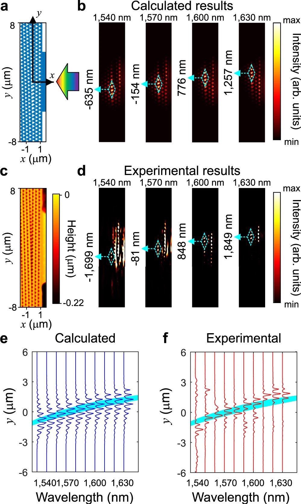
a The top view of the FDTD model, where coordinate axes are marked and light is incident from the waveguide. b The light intensity distributions (|E|2) of the calculated results for different wavelengths. c The topographic image of the sample. The color denotes the height of the surface of the sample. d The light intensity distributions of experimental results for different wavelengths. The comparison between interface intensity and projected bands for calculated (e) and experimental (f) results. In b, d, the position with maximal intensity is marked by the cyan dashed rhombuses, and the corresponding y coordinates are marked in the left. The wavelength of incident light is marked on the top of each figure. © Lu, C., Hu, X., Wang, C. et al. (2022)
Research Findings
Ultra-compact size on-chip topological rainbow nanophotonic devices were fabricated successfully by incorporating a synthetic dimension into a dielectric photonic crystal. The geometric parameters of the sample structure matched with the input waveguide geometry, while the central axis of the entire structure was aligned to the waveguide.
The interaction between the light and the AFM probe leads to the conversion of the near-field modes to back-guided modes in the input waveguide, which results in the formation of the modulated signal light.
Topological states of several wavelengths between the 1540 and 1630 nanometers/optical communication ranges were successfully slowed, separated, and trapped at various positions along the PC interface, forming a nanoscale topological rainbow on the SOI chip.
The rainbow effect was demonstrated directly and effectively using the homemade s-SNOM system for multiple optical lattice nanostructures. The group velocities were reduced to zero in different PC interface positions, where the slow-light effect of topological states was observed.
To summarize, the findings of this study demonstrated that the synthetic dimension-based topological nanophotonic device is well-suited for photonic chip integration as it can be implemented with purely dielectric materials. Additionally, the study also offers an avenue for implementing on-chip topological nanophotonic devices beyond the band topology of the structure, such as achieving non-zero Chern numbers in dielectric systems.
Reference
Lu, C., Hu, X., Wang, C. et al. (2022) On-chip nanophotonic topological rainbow. Nature Communications. https://www.nature.com/articles/s41467-022-30276-w
Disclaimer: The views expressed here are those of the author expressed in their private capacity and do not necessarily represent the views of AZoM.com Limited T/A AZoNetwork the owner and operator of this website. This disclaimer forms part of the Terms and conditions of use of this website.